IEDM 2014 was held in the second week of December 2014 in San Francisco. The excitement is over now and the dust has settled. Last week, at my leisure, I was glancing through the conference proceedings and short course material from IEDM 2014, when a slide from the 3DIC short course caught my attention. The slide presented below gives… Read More
Electronic Design Automation
STMicro to Showcase Turnkey NFC Design at MWC
Near-field communication (NFC) technology is finally realizing its potential, thanks to the impetus provided by Apple Pay, and it’s becoming evident from the pre-Mobile World Congress (MWC) buzz coming from several makers of chips, smartphones and wearable devices.
Among the companies displaying NFC products at the 2015 … Read More
Faster ECOs Using Formal Analysis
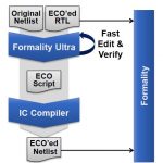
Your latest SoC has just begun the tape-out process and then marketing comes back with a small update to the specification to make your design more competitive, or maybe your regression tests just found a minor bug in a single IP block that needs to be fixed. Should you go back in your design flow, change the RTL source code and then completely… Read More
Mentor 2014 Results
Yesterday Mentor announced their quarterly results. Since their financial year is not aligned with the calendar year, this was also the end of their fiscal 2015. The quarter was an all-time record with revenues of $439M and (non-GAAP) EPS of $1.09. The year was also an all-time record with revenues of $1.24B and EPS of $1.77. Half… Read More
Atmel’s new car MCU tips imminent SoC journey
The automotive industry has reached a new era marked by giant initiatives like infotainment, connected car and semi-autonomous vehicles. And no one seems more excited than the MCU guys who have been a part and parcel of in-car electronics for the past two decades. However, the humble microcontroller is going through a profound… Read More
Got FPGA Timing Closure Problems?
I had a meeting with Harn Hua Ng, the CEO of Plunify, a couple of weeks ago. They are an EDA company that I’d never heard of. Partially that is because they only play in the FPGA space, a country I visit less frequently than SoC land. Plus, they are based in Singapore, a country I have only been to a couple of times in my life.
Plunify… Read More
Who Leads Semiconductor Innovation?
Semiconductor business is highly dependent on technology and that changes very rapidly in the semiconductor space. It’s important to recognize the importance of research and innovation activities in this space. In my last article on 7nm technology node, one respondent commented, very rightly, “It’s important to have competition… Read More
Vietnam: Rising Star in Electronics
I recently returned from a trip to Southeast Asia, including Vietnam. The trip was for pleasure, not business, but I could not help but notice the boom in economic activity. The coastal cities of Hai Phong, Da Nang and NHA Trang were trying to outdo each other in building hotels, bridges and amusement parks – largely to cater to foreign… Read More
A Brief History of CLKDA: Every Picosecond Counts Below 28nm
One thing to point out is that the CLK of CLKDA are the initials of the founders, they are not focused on clocks! I’m sure you can guess what DA stands for, although it is also the last two letters of the fourth founder’s name.
They have been in existence since 2005, backed by Atlas Ventures and Morgenthaler. They are headquartered… Read More
High Level Synthesis Gets Stronger
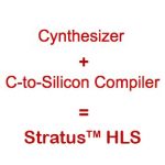
High Level Synthesis (HLS) tools have been around for at least two decades now, and you may recall that about one year ago Cadence acquired Forte. The whole promise of HLS is to provide more design and verification productivity by raising the design abstraction from RTL code up to SystemC, C or C++ code. With any acquisition it is natural… Read More


Silicon Insurance: Why eFPGA is Cheaper Than a Respin — and Why It Matters in the Intel 18A Era