You are currently viewing SemiWiki as a guest which gives you limited access to the site. To view blog comments and experience other SemiWiki features you must be a registered member. Registration is fast, simple, and absolutely free so please,
join our community today!
WP_Term Object
(
    [term_id] => 157
    [name] => EDA
    [slug] => eda
    [term_group] => 0
    [term_taxonomy_id] => 157
    [taxonomy] => category
    [description] => Electronic Design Automation
    [parent] => 0
    [count] => 4440
    [filter] => raw
    [cat_ID] => 157
    [category_count] => 4440
    [category_description] => Electronic Design Automation
    [cat_name] => EDA
    [category_nicename] => eda
    [category_parent] => 0
    [is_post] =>
)
FinFETs have brought a lot of good things to design – higher performance, higher density and lower leakage power – promising to extend Moore’s law for a least a while longer. But inevitably with new advances come new challenges, especially around optimizing for power integrity in these designs.
One of these challenges is… Read More
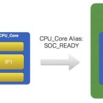
How can large SOC projects effectively integrate sub blocks and IP into a stable version for release or internal development? The person responsible for integrating SOC sub blocks into a validated configuration for release has a difficult task. Usually there are many sub-blocks, each undergoing their own development. There… Read More
The design of parallel interfaces is supposed to be (comparatively) easy — e.g., follow a few printed circuit board routing guidelines; pay attention to data/clock/strobe signal lengths and shielding; ensure good current return paths (avoid discontinuities); match the terminating resistances to the PCB trace impedance;… Read More
Hardware emulators and FPGA-based prototyping systems are descendants of the same ancestor. The Quickturn Systems Rapid Prototype Machine (RPM) introduced in May 1988 brought an array of Xilinx XC3090 FPGAs to emulate designs with hundreds of thousands of gates. From there, hardware emulators and FPGA-based prototyping … Read More
I recently had the opportunity to chat with Anirudh Devgan, senior vice president and general manager at Cadence, who leads the Digital and Signoff Group. We discussed recent product development initiatives at Cadence, and talked about future EDA and semiconductor market opportunities. His insights and comments were keen … Read More
2015 will be remembered as the year when chip-package-system (CPS) physical co-design and electrical/thermal analysis methodologies took center stage.… Read More
In last 3 decades of semiconductor market, the largest growth in IC sales was at 33% in 2010. At that time global recession had started due to financial crisis and in 2009 oil prices fell more than 30%. It appeared that oil prices were negatively correlated with semiconductor market growth. Today again there is another sharp decline… Read More
When technology advances, complexities increase and data size becomes unmanageable. Fresh thinking and a new environment for automation are needed to provide the required increase in productivity. Specifically in case of circuit simulation of advanced-node analog designs, where precision is paramount and a large number… Read More
About 35 years ago the first commercial SPICE circuit simulators emerged and they were quickly put to work helping circuit designers predict the timing and power of 6um NMOS designs. Then we had to limit our circuit simulations to just hundreds of transistors and interconnect elements to fit into the RAM and complete simulation… Read More
With the growth in streaming video and the promises of 50 billion IoT gadgets making our lives oh-so-much better, there is an alarming demand for online computational horsepower and bandwidth.
Why alarming? In 2014, data centers in the United States consumed approximately 100 billion kilowatt hours (kWh) of energy. According… Read More


Musk’s Orbital Compute Vision: TERAFAB and the End of the Terrestrial Data Center