You are currently viewing SemiWiki as a guest which gives you limited access to the site. To view blog comments and experience other SemiWiki features you must be a registered member. Registration is fast, simple, and absolutely free so please,
join our community today!
WP_Term Object
(
    [term_id] => 157
    [name] => EDA
    [slug] => eda
    [term_group] => 0
    [term_taxonomy_id] => 157
    [taxonomy] => category
    [description] => Electronic Design Automation
    [parent] => 0
    [count] => 4441
    [filter] => raw
    [cat_ID] => 157
    [category_count] => 4441
    [category_description] => Electronic Design Automation
    [cat_name] => EDA
    [category_nicename] => eda
    [category_parent] => 0
    [is_post] =>
)
This year is shaping up to be an inflection point, when multi-die packaging technology will experience tremendous market growth. Advanced 2.5D/3D package offerings have been available for several years, utilizing a variety of technologies to serve as the package substrate, interposer material for embedding die micro-bump… Read More
I was born in 1957, the same year that the Soviets launched the first satellite into Earth orbit, officially starting the Space Race between two global super powers. Today there are many countries engaged in space research and I just read about how engineers at IEAv (Institute for Advanced Studies) in Brazil did their IC design optimization… Read More
Improvements in SRAM Yield Variation Analysisby Tom Dillinger on 03-27-2016 at 12:00 pmCategories: EDA, Solido
The design of an SRAM array requires focus on the key characteristics of readability, writeability, and read stability. As technology scaling has enabled the integration of large (cache) arrays on die, the sheer number of bitcells has necessitated a verification methodology that focuses on “statistical high-sigma” variation… Read More
Not only are foundries continuing to introduce processes at new advanced nodes, they are frequently updating or adding processes at existing nodes. There are many examples that illustrate this well. TSMC now has 16FF, 16FF+ and now 16FFC. They are also announcing 10nm and 7nm processes. In addition, they are going back to older… Read More
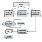
At DVCon I sat in on a series of talks on using higher-level abstraction for design, then met Adam Sherer to get his perspective on progress in bringing SystemC to the masses (Adam runs simulation-based verification products at Cadence and organized the earlier session). I have to admit I have been a SystemC skeptic (pace Gary Smith)… Read More
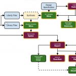
Whether or not in the past you believed all the of rhetoric about exploding design complexity in SOC’s, today there can be no debate that SOC size and complexity is well beyond something that can be managed without some kind of design management system. As would be expected, development of most larger designs relies on a data management… Read More
The intricacies of analog IP circuit design have always required special consideration during physical layout. The need for optimum device and/or cell matching on critical circuit topologies necessitates unique layout styles. The complex lithographic design rules of current FinFET process nodes impose additional restrictions… Read More
NPR had an interesting guest this morning: Edward Luce, author of “Time to Start Thinking: America in the Age of Descent”. I’m not about to turn SemiWiki into a politics blog, but there is some precedent in the technology business. I’ve caught myself saying more than once recently that “Motorola is no longer the company I worked 14… Read More
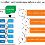
Imagine being able to use any combination of EDA vendor tools for schematic capture, SPICE circuit simulation, layout editing, place & route, DRC, LVS and extraction. On the foundry side, how about creating just a single Process Development Kit (PDK), instead of vendor-specific kits. Well, this is the basic premise of a recent… Read More
We might wish that all our design automation needs could be handled by pre-packaged vendor tool features available at the push of a button, but that never was and never will be the case. In the language of crass commercialism, there may be no broad market for those features, even though you consider that analysis absolutely essential.… Read More


Musk’s Orbital Compute Vision: TERAFAB and the End of the Terrestrial Data Center