You are currently viewing SemiWiki as a guest which gives you limited access to the site. To view blog comments and experience other SemiWiki features you must be a registered member. Registration is fast, simple, and absolutely free so please,
join our community today!
WP_Term Object
(
    [term_id] => 157
    [name] => EDA
    [slug] => eda
    [term_group] => 0
    [term_taxonomy_id] => 157
    [taxonomy] => category
    [description] => Electronic Design Automation
    [parent] => 0
    [count] => 4441
    [filter] => raw
    [cat_ID] => 157
    [category_count] => 4441
    [category_description] => Electronic Design Automation
    [cat_name] => EDA
    [category_nicename] => eda
    [category_parent] => 0
    [is_post] =>
)
We recently saw both Apple and Samsung introduce new smart phones, and realize that the annual race to introduce sophisticated devices that are attractive and differentiated is highly competitive. If either of these companies misses a market window then fortunes can quickly change. SoCs with billions of transistors like smart… Read More
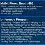
Next week is ARM TechCon which is one of my favorite conferences (SemiWiki is an event partner). This year is lucky number thirteen for ARM TechCon and it includes more than sixty hours of sessions plus more than one hundred ARM partners in the exposition. I will be signing free copies of our new book “Custom SoCs for IoT: Simplified”… Read More
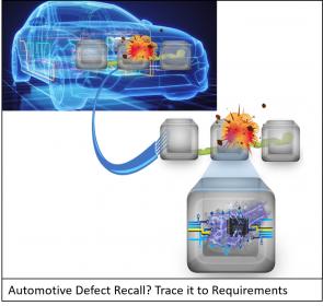
When it comes to safety and automotive systems, ISO 26262 is the standard by which system vendors are judged. As with all things the devil is in the details. To be compliant to the standard, design teams must have a well-defined and rigorous design and validation process in place that copiously documents all the requirements of their… Read More
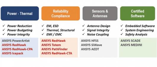
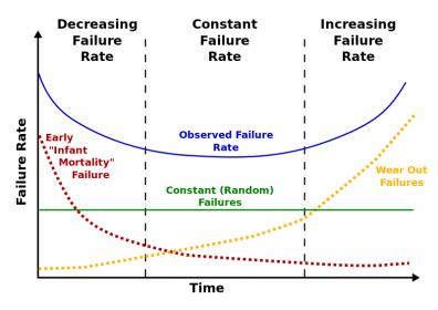
Ansys recently hosted a webinar on reliability signoff for FinFET-based designs, spanning thermal, EM, ESD, EMC and aging effects. I doubt you’re going to easily find a more comprehensive coverage of reliability impact and analysis solutions. If you care about reliability in FinFET designs, you might want to check out this webinar.… Read More
Magillem is hosting a user group meeting on October 26th at The Pad in Sunnyvale. User Group meetings are always educational; this one should be especially so for a number of reasons, not least of which is the keynote topic: Expert Systems for Experts.
REGISTER HERE for the meeting in Sunnyvale on October 26[SUP]th[/SUP] from 10:00am… Read More
ANSYS and TSMC will be co-presenting at ARM TechCon on Multiphysics Reliability Signoff for Next Generation Automotive Electronics Systems. The event is on Thursday October 26th, 10:30am-11:20am in Grand Ballroom B.
You can get a free Expo pass which will give you access to this event HERE and see the session page for the event … Read More
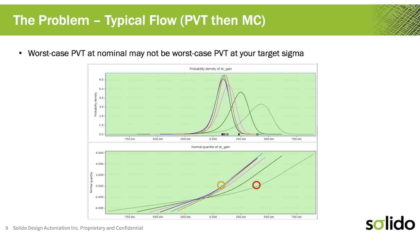
TSMC held its Open Innovation Platform Forum the other week on September 13[SUP]th[/SUP]. Each year the companies that exhibit at this event choose to highlight their latest technology. One of the most interesting presentations that I received during the event was from Solido. In recent years they have produced a number of groundbreaking… Read More
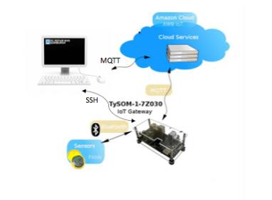
A piece of learning we all seem to have gained from practical considerations of IoT infrastructure is that no, it doesn’t make sense to ship all the data from an IoT edge device to the cloud and let the cloud do all the computational heavy lifting. On the face of it that idea seemed good – all those edge devices could be super cheap (silicon… Read More
My educational background is Electrical Engineering and I’ve learned a lot since starting in the industry back in 1978 while working on bipolar, NMOS and CMOS technology, designing DRAM, data controller and GPU devices. I continue to learn about the semiconductor industry through daily reading and attending trade shows… Read More
I mentioned back in June that Synopsys had launched a blog on formal verification, intended to demystify the field and provide help in understanding key concepts. It’s been a few months, time to check in on some of their more recent posts.
First up, it feels like they are finding their groove. Relaxed style, useful topics but now with… Read More


Musk’s Orbital Compute Vision: TERAFAB and the End of the Terrestrial Data Center