You are currently viewing SemiWiki as a guest which gives you limited access to the site. To view blog comments and experience other SemiWiki features you must be a registered member. Registration is fast, simple, and absolutely free so please,
join our community today!
WP_Term Object
(
    [term_id] => 157
    [name] => EDA
    [slug] => eda
    [term_group] => 0
    [term_taxonomy_id] => 157
    [taxonomy] => category
    [description] => Electronic Design Automation
    [parent] => 0
    [count] => 4441
    [filter] => raw
    [cat_ID] => 157
    [category_count] => 4441
    [category_description] => Electronic Design Automation
    [cat_name] => EDA
    [category_nicename] => eda
    [category_parent] => 0
    [is_post] =>
)
When I first started doing IC design back in 1978 we had hierarchical designs, and that was doing a relatively simple 16Kb DRAM chip with only 32,000 transistors using 6um (aka 6,000 nm) design rules. SoC designs today make massive use of hierarchy at all levels of IC design: IC Layout, transistor netlist, gate level netlist, RTL … Read More
Layout parasitic extraction (LPE) has three primary goals – accuracy, capacity, and throughput. Traditionally, LPE tools have offered two methods for capacitance derivation, with tradeoffs on these goals:… Read More
SEMI is a worldwide organization with local chapters like the one here in Oregon, where I attended a recent half-day presentation by several industry experts on the topic – Globalization, How it shapes the Semiconductor industry:
- Michael Chen, Director, Mentor – A Siemens Business
- John Brewer, CEO, Amorphyx
- Ed
…
Read More
Schematics are still the lynchpin of analog design. In the time that HDL’s have revolutionized digital design, schematics have remained drawn and used much as they have been for decades. While the abstraction of HDL based designs has made process and foundry porting relatively straightforward, porting schematic based designs… Read More
While it’s interesting to hear a tool-vendor’s point of view on the capabilities of their product, it’s always more compelling to hear a customer/user point of view, especially when that customer is NVIDIA, a company known for making monster chips.
A quick recap on the concept. At 7nm, operating voltages are getting much closer… Read More
I was driving recently on highway 87 (San Jose) and wanted to merge left. I checked my side-mirror, checked the blind-spot detector, saw no problems and started to move over – and quickly swerved back when a car shot by on my left. What went wrong? My blind-spot detection, a primary feature in ADAS (advanced driver assistance systems,… Read More
I say finally because it was a long time coming… almost ten years to be exact. I started doing business development work for both Solido and Berkeley Design Automation about ten years ago and have been trying to put them together ever since. The synergy was obvious, like peanut butter and jelly. In fact, this is my third time … Read More
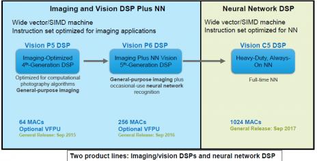
Cadence has recently announced two key design-in for their Vision DSP IP family: MediaTek’s Helio P30 integrates the Tensilica Vision P5 DSP and HiSilicon has selected the Cadence® Tensilica® Vision P6 DSP for its 10nm Kirin 970 mobile application processor. The Kirin 970 being integrated into Huawei’s new Mate 10 Series mobile… Read More
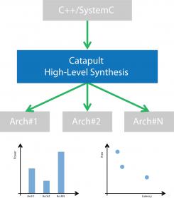
The complexity of silicon chips is exploding. Actually, it has been growing at a tremendous speed for decades. So far, the semiconductor industry has been successful at providing new ways to master new levels of complexity, over and over again.
Standardizing hardware platforms, using higher-level languages with a knowledge… Read More
Automotive markets have added pressure on semiconductor/systems design through demand for ISO26262 compliance – this we all know. But they have also changed the mix of important design types. Once class of design that has become very significant in ADAS, and ultimately autonomous applications, is image signal processing (ISP).… Read More


Musk’s Orbital Compute Vision: TERAFAB and the End of the Terrestrial Data Center