You are currently viewing SemiWiki as a guest which gives you limited access to the site. To view blog comments and experience other SemiWiki features you must be a registered member. Registration is fast, simple, and absolutely free so please,
join our community today!
WP_Term Object
(
    [term_id] => 157
    [name] => EDA
    [slug] => eda
    [term_group] => 0
    [term_taxonomy_id] => 157
    [taxonomy] => category
    [description] => Electronic Design Automation
    [parent] => 0
    [count] => 4441
    [filter] => raw
    [cat_ID] => 157
    [category_count] => 4441
    [category_description] => Electronic Design Automation
    [cat_name] => EDA
    [category_nicename] => eda
    [category_parent] => 0
    [is_post] =>
)
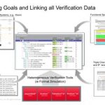
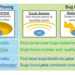
One of the great aspects of modern hardware verification is that we keep adding new tools and methodologies to support different verification objectives (formal, simulation, real-number simulation, emulation, prototyping, UVM, PSS, software-driven verification, continuous integration, …). One of the downsides to this… Read More
When it comes to building edge devices for the internet-of-things (IoT), you don’t want to have to break the bank to prototype an idea before diving into the deep water. At the same time, if your idea is to shrink an edge device down to it’s smallest dimensions, lowest power and lowest cost, you really want to be able to prototype your… Read More
Synopsys has been quite active lately in their messaging around formal verification. One such event at DVCon this year was a tutorial on some of the more advanced techniques/ methodologies that are accessible to formal teams, mostly presented by customers, though opened by a Synopsys presentation. The tutorial covered so many… Read More
At the Silicon Valley SNUG 2018, Synopsys Chairman and co-CEO Dr. Aart de Geuss gave his keynote speech addressing attendees on how far we have evolved, and at times encountered the aha factor that helps propel us to the next level. He explored trends as well as the current state of his company solution offerings.
Moore’s Law, Digital… Read More
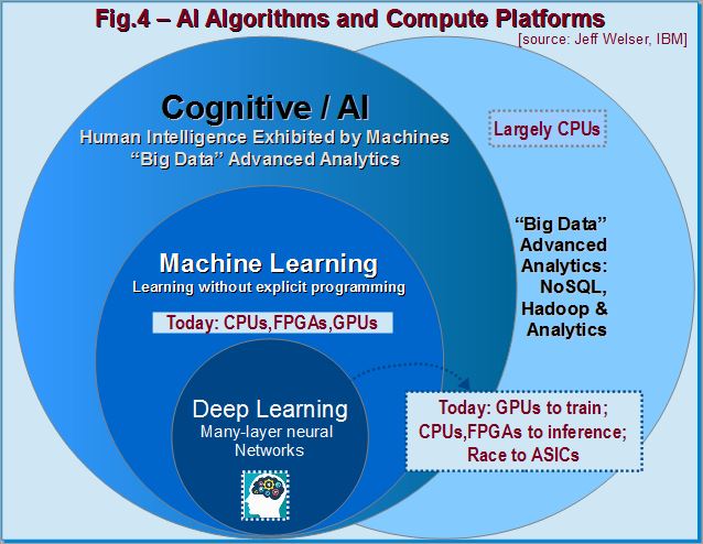
Adding color to the talks, Dr. Jeff Welser, VP and IBM Almaden Research Lab Director showed how AI and recent computing resources could be harnessed to contain data explosion. Unstructured data growth by 2020 would be in the order of 50 Zetta-bytes (with 21 zeros). One example, the Summit supercomputer developed by IBM for use at… Read More
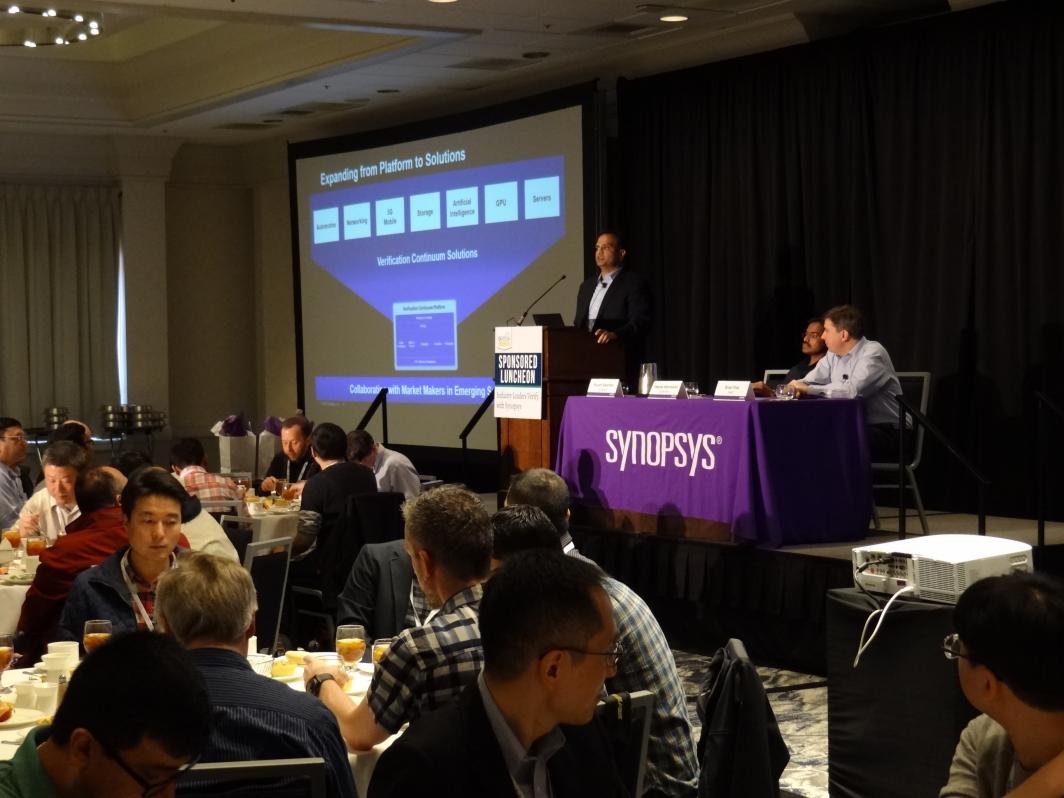
Synopsys hosts a regular lunch at DVCon each year (at least over the last few years I have checked), a nice meal and a show, opening a marketing update followed by 2-3 customer presentations on how they use Synopsys verification in their flows. This year’s event was moderated by Piyush Sancheti from Synopsys Verification marketing… Read More
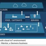
For those of you who wondered at the logic behind Siemens acquisition of Mentor Graphics last year, look no further than a recent announcement by Mentor, now a Siemens business, regarding the release of their new Mentor Embedded IoT Framework (MEIF). To help connect the dots, we need to back up a bit and review a few things about how… Read More
Designers spend a lot of time looking at their layouts in 2D. This is done naturally because viewing in 2D is faster and simpler than in 3D. It helps that humans are good at extrapolating from 2D to 3D. Analysis software, such as extraction software also spend a lot of time looking at layouts in 2D. While this is fine for approximate results,… Read More
This year I got a chance to talk with Cadence at DVCon on a whole bunch of topics, so expect a steady stream of blogs over the next couple of months. First up was an update from Pete Hardee (Director of Product Management) on, surprise, surprise, formal verification. I’m always trying to learn more about this space, so I picked a couple… Read More
The second panel is about system coverage and big data. Coverage metrics have been used to gauge the quality of verification efforts during development. At system level, there are still no standardized metrics to measure full coverage. The emergence of PSS, better formal verification, enhanced emulation and prototyping techniques… Read More


Musk’s Orbital Compute Vision: TERAFAB and the End of the Terrestrial Data Center