You are currently viewing SemiWiki as a guest which gives you limited access to the site. To view blog comments and experience other SemiWiki features you must be a registered member. Registration is fast, simple, and absolutely free so please,
join our community today!
WP_Term Object
(
    [term_id] => 19172
    [name] => Chiplet
    [slug] => chiplet
    [term_group] => 0
    [term_taxonomy_id] => 19172
    [taxonomy] => category
    [description] =>
    [parent] => 0
    [count] => 195
    [filter] => raw
    [cat_ID] => 19172
    [category_count] => 195
    [category_description] =>
    [cat_name] => Chiplet
    [category_nicename] => chiplet
    [category_parent] => 0
    [is_post] =>
)
As semiconductor industry folks know, Synopsys is a behemoth of a company. At $5.84B in FY2023 revenue (FY Nov-Oct), approximately 20,000 employees and a market cap of about $74B, it leads the silicon-to-systems design solutions space within the industry. From humble beginnings in 1986 as a disruptive startup, the company has… Read More
Matt develops go-to-market strategies for Samtec’s Silicon to Silicon solutions. Over the course of 20+ years, he has been a leader in design, technical sales and marketing in the telecommunications, medical and electronic components industries. It has been an honor working with Matt and his team for the last 3 years and I value… Read More
There is a lot being said about Intel getting the lead back from TSMC with their 18A process. Like anything else in the semiconductor industry there is much more here than meets the eye, absolutely.
From the surface, TSMC has a massive ecosystem and is in the lead as far as process technologies and foundry design starts but Intel is … Read More
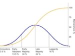
If we look at the semiconductor industry expansion during the last 25 years, adoption of design IP in every application appears to be one of the major factors of success, with silicon technology incredible development by a x100 factor, from 250nm in 2018 to 3nm (if not 2nm) in 2023. We foresee the move to chiplet-based architecture… Read More
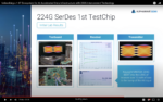
In the rapidly evolving landscape of artificial intelligence (AI) and data-intensive applications, the demand for high-performance interconnect technologies has never been more critical. Even the 100G Interconnect is already not fast enough for infrastructure applications. AI applications, with their massive datasets… Read More
First, a quick definition. By “structured assembly,” I mean the collection of tools to support IP packaging with standardized interfaces, SoC integration based on those IPs together with bus fabric and other connectivity hookups, register definition and management in support of hardware/software interface definition, … Read More
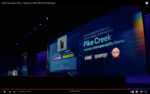
Intel recently made headlines when CEO Pat Gelsinger unveiled the world’s first UCIe interoperability test chip demo at Innovation 2023. The test chip built using advanced packaging technology is codenamed Pike Creek and is used to demonstrate interoperability across chiplets designed by Intel and Synopsys. More details … Read More
S2C has been successfully delivering rapid SoC prototyping solutions since 2003 with over 600 customers, including 6 of the world’s top 10 semiconductor companies. I personally have been involved with the prototyping market for a good part of my career and know S2C intimately.
S2C is the leading independent global supplier… Read More
While the leap from traditional SoC/IC designs to Three-Dimensional Integrated Circuits (3DICs) designs brings new benefits and opportunities, it also introduces new challenges. The benefits include performance, power efficiency, footprint reduction and cost savings. The challenges span design, verification, thermal… Read More
One of the most promising advancements in the semiconductor field is the development of 3D Integrated Circuits (3D ICs). 3D ICs enable companies to partition semiconductor designs and seamlessly integrate silicon Intellectual Property (IP) at the most suitable process nodes and processes. This strategic partitioning yields… Read More


Musk’s Orbital Compute Vision: TERAFAB and the End of the Terrestrial Data Center