You are currently viewing SemiWiki as a guest which gives you limited access to the site. To view blog comments and experience other SemiWiki features you must be a registered member. Registration is fast, simple, and absolutely free so please,
join our community today!
WP_Term Object
(
    [term_id] => 23705
    [name] => 3D IC
    [slug] => 3dic
    [term_group] => 0
    [term_taxonomy_id] => 23705
    [taxonomy] => category
    [description] =>
    [parent] => 0
    [count] => 120
    [filter] => raw
    [cat_ID] => 23705
    [category_count] => 120
    [category_description] =>
    [cat_name] => 3D IC
    [category_nicename] => 3dic
    [category_parent] => 0
    [is_post] =>
)
By Todd Burkholder and Per Viklund, Siemens EDA
The landscape of advanced IC packaging is rapidly evolving, driven by the imperative to support innovation on increasingly complex and high-capacity products. The broad industry trend toward heterogeneous integration of diverse die and chiplets into advanced semiconductor… Read More
AI’s rapid expansion is reshaping semiconductor design. The compute and I/O needs of modern AI workloads have outgrown what traditional SoC scaling can deliver. As monolithic dies approach reticle limits, yields drop and costs rise, while analog and I/O circuits gain little from moving to advanced process nodes. To sustain … Read More
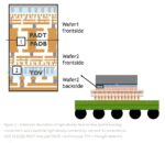
In the rapidly evolving landscape of semiconductor technology, imec’s recent breakthroughs in wafer-to-wafer hybrid bonding and backside connectivity are paving the way for CMOS 2.0, a paradigm shift in chip design. Introduced in 2024, CMOS 2.0 addresses the limitations of traditional CMOS scaling by partitioning… Read More
Now that the dust has settled let’s talk more about TSMC’s Open Innovation Platform. Launched in 2008, OIP represents a groundbreaking collaborative model in the semiconductor industry. Unlike IDMs that controlled the entire supply chain, OIP fosters an “open horizontal” ecosystem uniting TSMC… Read More
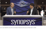
At the AI Infra Summit 2025, Synopsys showed how artificial intelligence has become inseparable from the process of creating advanced silicon. The company’s message was clear: AI is an end-to-end engine that drives every phase of chip development. Three Synopsys leaders illustrated this from distinct vantage points. Godwin… Read More
Synopsys has deepened its collaboration with TSMC certifying the Ansys portfolio of simulation and analysis tools for TSMC’s cutting-edge manufacturing processes including N3C, N3P, N2P, and A16. This partnership empowers chip designers to perform precise final checks on designs, targeting applications in AI acceleration,… Read More
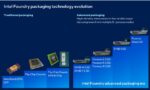
In the rapidly evolving landscape of semiconductor manufacturing, the demand for processors that handle increasing workloads while maintaining power efficiency and compact form factors has never been higher. Intel’s Foveros 2.5D packaging technology emerges as a pivotal innovation, enabling denser die integration… Read More
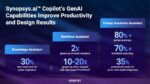
In the fast-paced semiconductor industry Synopsys has redefined EDA with its Synopsys.ai Copilot, a generative AI tool. Since its launch in November 2023, and yes I was at the launch and very skeptical, Copilot has evolved to address the industry’s growing design complexity and projected 15-30% workforce gap by 2030. Let’s… Read More
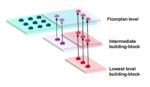
Everyone knows design complexity is exploding. What used to be difficult is now bordering on impossible. While design and verification challenges occupy a lot of the conversation, the problem is much bigger than this. The new design and manufacturing challenges of 3D innovations and the need to coordinate a much more complex … Read More
Welcome to the second half of a very exciting year in semiconductors. While Intel and Samsung Foundry have made quite a few headlines, TSMC continues to execute flawlessly at 3nm and 2nm. With the TSMC OIP Ecosystem Forums starting later this month let’s take a look at how we got to where we are today.
The TSMC OIP Ecosystem Forum… Read More


Chemical Origins of Environmental Modifications to MOR Lithographic Chemistry