SOCs designed on advanced FinFET nodes like 7, 5 and 3nm call for silicon-validated physical analog IP for many critical functions. Analog blocks have always been node and process specific and their development has always been a challenge for SOC teams. Fortunately, there are well established and endorsed analog IP companies… Read More
Author: Tom Simon
Package Pin-less PLLs Benefit Overall Chip PPA
Executable Specifications Shorten Embedded System Development
Even though AI is being used to replace procedural coding for many embedded applications, there is still, and will be for a long time, code that is written manually to deal with complicated inputs to control connected systems. Even in AI based systems there are programmer coded steps for responses to AI identified inputs. All of … Read More
A Custom Layout Environment for SOC Design Closure
Throughout the process of physical design and verification there are many groups working on the design. Most often these groups are working independently or in parallel but separately, using their own specialized tools, such as P&R, DRC, custom layout, DFM, etc. At the end of the process there is an inevitable requirement… Read More
Fully Modeling the Semiconductor Manufacturing Process
A lot of folks in the semiconductor business are familiar with Dassault Systèmes because of their product life cycle management (PLM) products for IC design. They are, of course well known in other industries as well for their 3D modeling and simulation software. Over the years they have added capabilities and intelligence to … Read More
Obtaining Early Analog Block Area Estimates
I’ve written before about Pulsic’s Animate Preview software, which is extremely helpful in completing placement in analog blocks so that they are ready for routing. Analog design automation has always been a tough proposition, but Animate Preview looks like a promising tool, with practical benefits. Obtaining DRC clean placement… Read More
PCIe Gen 6 Verification IP Speeds Up Chip Development
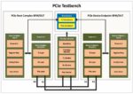
PCIe is a prevalent and popular interface standard that is used in just about every digital electronic system. It is used widely in SOCs and in devices that connect to them. Since it was first released in 2003, it has evolved to keep up with rapidly accelerating needs for high speed data transfers. Each version has doubled in throughput,… Read More
Driving PPA Optimization Across the Cubic Space of 3D IC Silicon Stacks
The move to true 3D IC, monolithic 3D SOC and 3D heterogeneous integration may require one of the most major design tool architecture overhauls since IC design tools were first developed. While we have been taking steps toward 3DIC with 2.5D designs with interposers, HBM, etc., the fundamental tools and flows remain intact in many… Read More
Siemens Offers Insights into Gate Level CDC Analysis
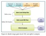
Glitches on clock domain crossing signals have always been a concern for chip designers. Now with increased requirements for reliability, renewed scrutiny is being given to find ways to identify these problems and fix them. In particular applications such as automotive electronics have given this added effort an impetus. Siemens… Read More
Die-to-Die Connections Crucial for SOCs built with Chiplets
If you ascribe to the notion that things move in circles, or concentrically, the move to die-to-die connectivity makes complete sense. Just as multi-chip modules (MCM) were the right technology decades ago to improve power, areas, performance and cost, the use of chiplets with die-to-die connections provides many advantages… Read More
RealTime Digital DRC Can Save Time Close to Tapeout
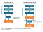
Over the years DRC tools have done an admirable job of keeping pace with the huge growth of IC design size. Yet, DRC runs for sign off on the full design using foundry rule decks take many hours to complete. These long run times are acceptable for final sign off, but there are many situations where DRC results are needed quickly when small… Read More


Tesla and Samsung Relationship Update