You are currently viewing SemiWiki as a guest which gives you limited access to the site. To view blog comments and experience other SemiWiki features you must be a registered member. Registration is fast, simple, and absolutely free so please,
join our community today!
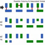
David Avercrombie of Mentor won the award for the best tutorial at the 2012 TSMC OIP for his presentation, along with Peter Hsu of TSMC, on Finding and Fixing Double Patterning Errors in 20nm. The whole presentation along with the slides is now available online here. The first part of the presentation is an introduction to double … Read More
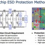
In Pune at the start of the month, Norman Chang, Ting-Sheng Ku, Jai Pollayil of Apache/Ansys and NVIDIA presented and ESD check methodologywith Fast Full-chip Static and Macro-level Dynamic Solutions . ESD stands for Elecro-Static Discharge and is basically injecting very high static voltages (think how your hand gets charged… Read More
I was asked to make some predictions about the EDA, semiconductor and electronic systems markets for 2013. I decided that it would be more fun to make some plausible predictions, some of which will be right, rather than go for anodyne predictions (“Cadence will acquire a couple of startups”) which are uninformative,… Read More
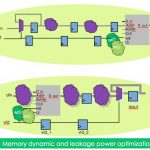
Sequential approaches to power reduction work well on logic implemented using standard cells. But part of every SoC, sometimes a very large part, is taken up with embedded memories for which alternative approaches are required. Not only do these memories occupy up to half of the area they also account for as much as 75% of the power… Read More
Global Design Closureby Paul McLellan on 01-09-2013 at 8:34 pmCategories: EDA
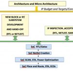
Satish Soman, chief solutions architect at Atrenta, was invited to give a presentation on Global Design Closure at the VLSI India conference in Pune at the start of this month. He talked about the need to close the gap between the typical SoC development methodology and what happens in reality.
SoCs are really put together in two … Read More
The current methodology in design in most companies, and certainly many of the biggest, is that front end RTL design is done by one team with a limited set of front-end design tools. This is then eventually passed off to the physical design team who run all the scripts, do the “real” synthesis, place & route and timing… Read More
Did you watch Atrenta’s holiday video (it’s only one minute)? Various Atrenta employees from all over the world wished you happy holidays in their own languages. Now Atrenta are having a competition. If you identify all the languages in the video then you can win an iPad Mini.
To enter the competition, or to view the … Read More
Next week it is the Consumer Electronics Show (CES) in Las Vegas and so there are announcements around the areas where consumer overlaps with semiconductor, which these days is primarily mobile. Then in February in Barcelona is Mobile World Congress, which is even more focused on mobile. Expect more announcementst there.
Currently… Read More
I didn’t attend the International Electronic Device Meeting (IEDM) earlier this month, but there have been a lot of reports on the inter webs especially about 20nm and 14nm processes. Some of this is really geeky stuff but I think that perhaps the most interesting thing I’ve read about is summarized in this chart:
This… Read More
A couple of weeks ago was the 3D Architectures for Semiconductor Integration and Packagingconference in Redwood City. Cadence presented the changes that they have been making to their tool flow to enabled 2.5D (interposer-based) and true 3D TSV-based designs. You know what TSV stands for by now right? Through-silicon-via, … Read More


Musk’s Orbital Compute Vision: TERAFAB and the End of the Terrestrial Data Center