
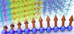
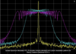
There is a revolution happening that is fueled by innovation in areas such as AI, IoT and autonomous driving. These new systems put incredible stress on next-generation semiconductor technology. Faster processing, higher density and lower latency must all be delivered with reduced power and thermal profiles. One technology… Read More

Author: Mike Gianfagna
Synopsys Brings Embedded Memory to the Future with its Flexible, IP-Based Compilers
Intel Presents the Final Frontier of Transistor Architecture at IEDM
IEDM was buzzing with many presentations about the newest gate-all-around transistor. Both Intel and TSMC announced processes based on nanosheet technology. This significant process innovation allows the fabrication of silicon RibbonFET CMOS devices, which promise to open a new era of transistor scaling, keeping Moore’s… Read More
TSMC Unveils the World’s Most Advanced Logic Technology at IEDM
There was a lot of discussion at IEDM about the coming shift to gate-all-around (GAA) transistor structures. This new device brings many benefits to continue device scaling, both at the monolithic device level as well as for multi-die design. The path to GAA is not simple, there are new material, process and design considerations… Read More
An Invited Talk at IEDM: Intel’s Mr. Transistor Presents The Incredible Shrinking Transistor – Shattering Perceived Barriers and Forging Ahead

IEDM turned 70 last week. This was cause for much celebration in the form of special events. One such event was a special invited paper on Tuesday afternoon from Intel’s Tahir Ghani, or Mr. Transistor as he is known. Tahir has been driving innovation at Intel for a very long time. He is an eyewitness to the incredible impact of the Moore’s… Read More
IEDM Opens with a Big Picture Keynote from TSMC’s Yuh-Jier Mii
The main program for the 70th IEDM opened on Monday morning in San Francisco with an excellent keynote from Dr. Yuh-Jier Mii, Executive Vice President and Co-Chief Operating Officer at TSMC. Dr. Mii joined TSMC in 1994. Since then, he has contributed to the development and manufacturing of advanced CMOS technologies in both fab
Synopsys Brings Multi-Die Integration Closer with its 3DIO IP Solution and 3DIC Tools

There is ample evidence that technologies such as high-performance computing, next-generation servers, and AI accelerators are fueling unprecedented demands in data processing speed with massive data storage, lower latency, and lower power. Heterogeneous system integration, more commonly called 2.5 and 3D IC design, … Read More
A Master Class with Ansys and Synopsys, The Latest Advances in Multi-Die Design

2.5D and 3D multi-die design is rapidly moving into the mainstream for many applications. HPC, GPU, mobile, and AI/ML are application areas that have seen real benefits. The concept of “mix/match” for chips and chiplets to form a complex system sounds deceptively simple. In fact, the implementation and analysis techniques required… Read More
How Breker is Helping to Solve the RISC-V Certification Problem
RISC-V cores are popping up everywhere. The growth of this open instruction set architecture (ISA) was quite evident at the recent RISC-V summit. You can check out some of the RISC-V buzz on SemiWiki here. While all this is quite exciting and encouraging, there are hurdles to face before true prime-time, ubiquitous application… Read More
MZ Technologies is Breaking Down 3D-IC Design Barriers with GENIO
3D-IC design can be both exciting and frustrating. It’s exciting because it opens a new world of innovation possibilities – opportunities that aren’t constrained by the rules of monolithic chip scaling. It can be frustrating because of the large array of complex technical challenges that must be overcome to make this new paradigm… Read More
One Thousand Production Licenses Means Silicon Creations PLL IP is Everywhere
If you sell sneakers, 1,000 pair is called a humble beginning. On the other hand, selling 1,000 licenses for specialized analog IP is a home run. Silicon Creations celebrated a home run for a critical piece of analog IP that finds its way into a diverse array of applications. Succeeding in so many markets is noteworthy, and I want … Read More


Musk’s Orbital Compute Vision: TERAFAB and the End of the Terrestrial Data Center