You are currently viewing SemiWiki as a guest which gives you limited access to the site. To view blog comments and experience other SemiWiki features you must be a registered member. Registration is fast, simple, and absolutely free so please,
join our community today!
Book Review – iWozby Daniel Payne on 03-12-2012 at 11:01 amCategories: General
I bought my first personal computer in 1979, it was a Radio Shack TRS-80 Model I with just 16KB of RAM, a BW monitor and casette tape for storage. The reason that I chose the Radio Shack over the Apple II was that it cost less, so I was always interested in Apple products and the engineers behind them since the early days. It was pure delight… Read More
Designing custom IP blocks is a challenge at the transistor-level and I wanted to learn what the recommended methodology and EDA tool flow was at Synopsys. They have a webinar that you can register for and it takes 30 minutes to learn what they have to say, or you can read a White Paper. If you cannot spare that much time, then my summary… Read More
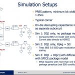
HSPICE users gathered in January 2012 at the HSPICE SIG(Special Interest Group) to talk about their experiences using this circuit simulator for a variety of IC and signal integrity issues. I wasn’t able to attend in person however I did watch the video and wanted to summarize what I heard:… Read More
My first chip design at Intel was a DRAM and we had a 5% yield problem caused by electromigration issues, yes, you can have EM issues even with 6um NMOS technology. We had lots of questions but precious few answers on how to pinpoint and eliminate the source of yield loss. Fortunately, with the next generation of DRAM quickly introduced… Read More
Nandu Bhagwan is CEO of GHz Circuits and has been designing PLL circuits used in ICs for the past 12 years. Mr. Bhagwan did a video interview with John Pierce of Cadence to talk about the challenges of PLL design.… Read More
How do I know if an AMS block is tuned for the process and will perform and yield acceptably?… Read More
Digital designers have used diff tools for years on their text-based HDL source code, but what about for the transistor-level IC designer, where is their diff tool for schematics or layout?… Read More
Ken Kundert while at Cadence developed: Spectre, Spectre RF, Verilog-A and Verilog-AMS. About 6 years ago he and Henry Chang left Cadence and created a consulting company called The Designers Guide.
… Read More
At DAC in 2011 I visited an EDA company called Silicon Frontline Technology because they offered some 3D field solver tools used to create the highest accuracy netlists that can then be simulated with a SPICE circuit simulator to predict timing, power and IR drop. A recent press release with X-FAB and Silicon Frontline looked interesting… Read More


Quantum Simulation Using Decision Diagrams. Innovation in Verification