





Next-gen AI accelerators, high-performance processors, and complex computing architectures depend heavily on advanced packaging. Bringing multiple dies, chiplets, high-bandwidth memory, and advanced interconnects together into a single 2.5D or 3D package yields massive performance gains. However, this design evolution introduces a massive roadblock to internal visibility.
As hardware packaging gets more intricate, tracking internal operations becomes a headache. These multi-die setups often mix components from different manufacturing processes. They rely on high-speed die-to-die interfaces and face extreme power and thermal stress.
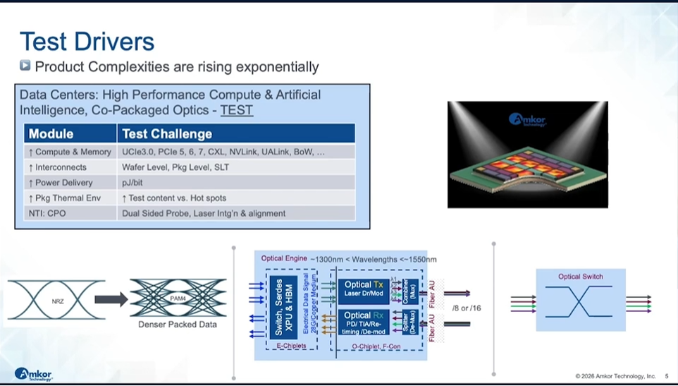
To make matters worse, finding a hardware defect gets exponentially more expensive the further a device moves down the production line. Because of this, the semiconductor industry desperately needs a fresh approach to testing and hardware reliability. We need systems that offer deep insights into the silicon itself, turning raw data into clear, actionable intelligence.
Vineet Pancholi from Amkor Technology and Nir Sever from proteanTecs, recently hosted a webinar on this very topic. Vineet is Senior Director, Manufacturing & Test and Nir is Senior Director of Business Development at their respective companies.
The Problem: Escalating Complexity
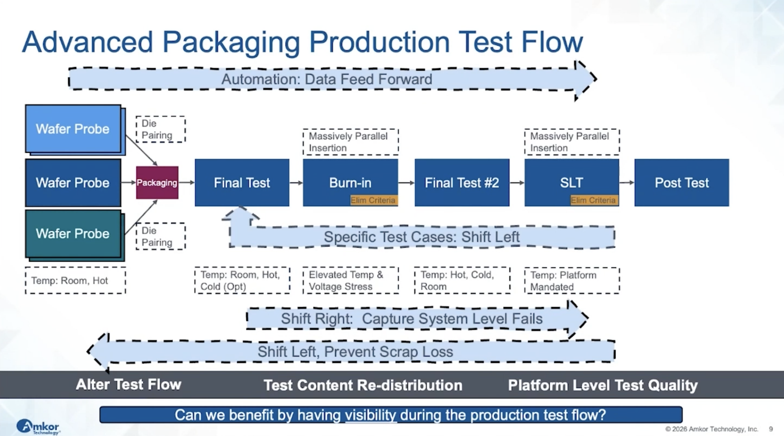
Larger die and package sizes invariably mean longer test times and higher testing costs. Spotting a defect only after final assembly means time and money spent on a flawed product. This highlights the need for early detection, to improve compound yield and keep scrap rates low.
Traditional pass/fail testing cannot catch subtle signs of marginal performance or latent defects. Die-to-die interconnects add another layer of trouble. Internal interfaces often run at data rates far beyond what package-level tester interfaces can handle, making it very difficult to map their actual behavior.
Power delivery and thermal control are also hitting a wall. Overall exponential increase in power consumption, spiking power and thermal densities and complex power delivery and heat dissipation, bring too many unstable variables into the mix, threatening long-term reliability.
Just knowing whether a chip passes a basic test is no longer enough. The industry must deeply analyze how a chip behaves under stress and also verify whether that behavior matches real-world performance expectations.
Rethinking the Testing Paradigm
Fixing these issues takes more than just stacking extra steps onto the test line. It demands deeper visibility, faster decision-making, and unprecedented access to real-time data from deep inside the hardware.
- Moving Beyond Binary Pass/Fail: Manufacturers need rich, granular metrics. Parametric data exposes exactly how an individual die is holding up, revealing subtle performance variations that traditional testing thresholds completely overlook.
- Shifting Decisions Upstream: Quality control must happen much earlier in the manufacturing timeline. Because every single component affects the final yield of a multi-die package, catching borderline components before assembly is critical. This “shift-left” approach ensures smarter Known Good Die (KGD) vetting, stopping subpar chips from entering the final packaging stages.
- Adapting Test Access to Modern Architectures: Test protocols have to keep pace with new silicon designs. New die-to-die standards and Design-for-Test (DFX) methods are helping close the gap in complex multi-die environments. Relying on interfaces like UCIe, PCIe, CXL, and NVLink is key for modern testing strategies, in conjunction with advanced DFX, streaming scan networks, and expanded test bandwidth.
- Tracking Performance Long After Production: True visibility doesn’t stop at the factory gate. Once deployed in real-world environments, these devices handle constantly shifting workloads, voltage swings, and thermal spikes. Continuous tracking offers vital clues about wear, long-term reliability, and hardware optimization.
In short, the industry has to stop viewing testing as a series of isolated checkups and start tracking hardware behavior across its entire operational lifespan.
The Solution: Deep Silicon Visibility
This is precisely the challenge proteanTecs addresses. By embedding dedicated monitoring agents and sensors directly onto the chip architecture, proteanTecs captures high-fidelity “deep data.” This includes precise parametric details tracking how the silicon reacts during initial production runs and live mission-mode operations. Specialized software analytics then process this raw telemetry into highly actionable intelligence.
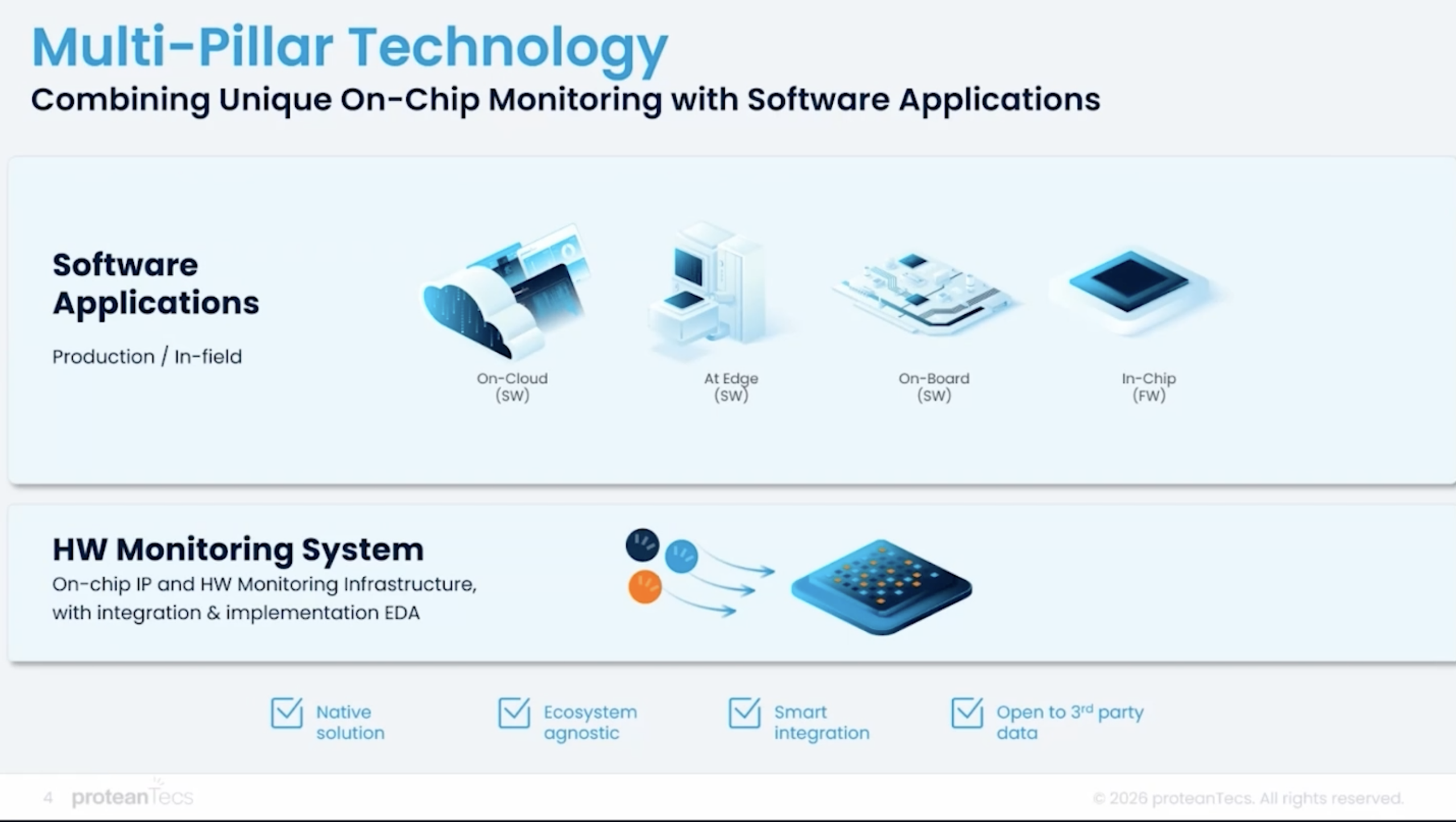
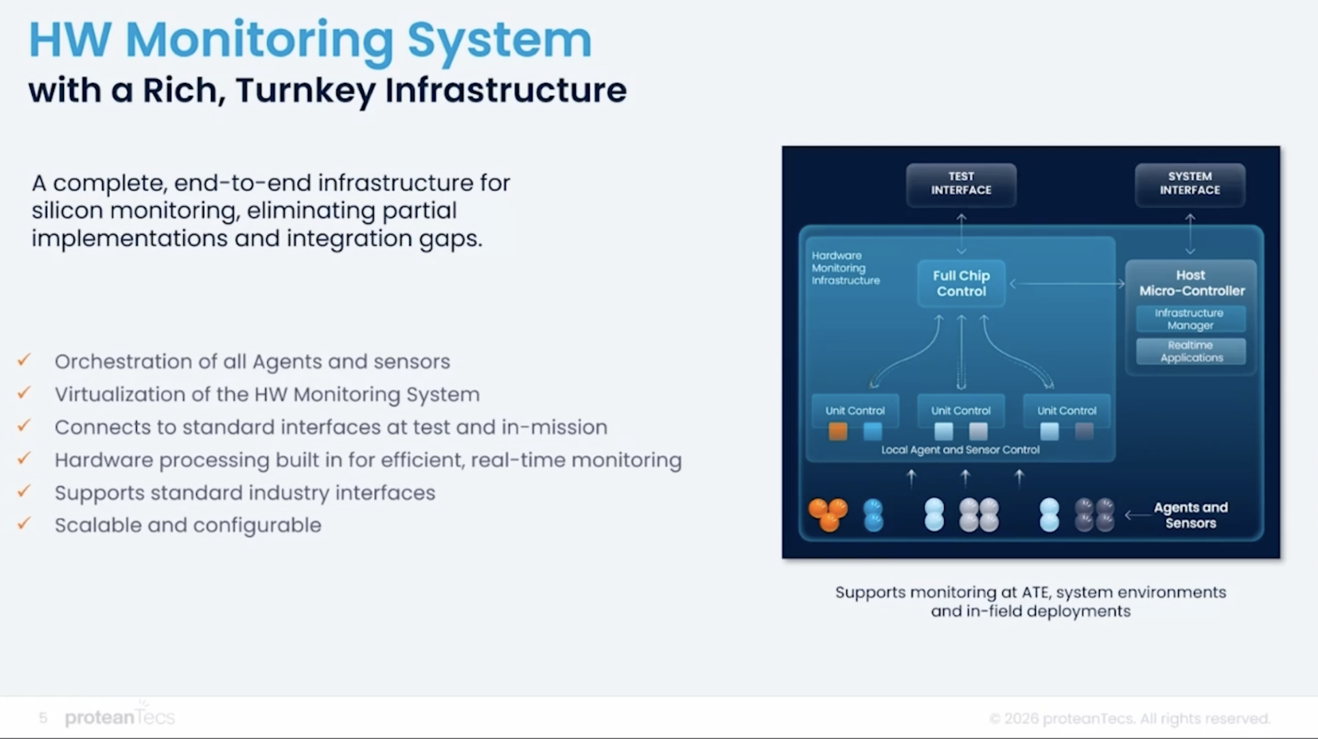
This approach elevates hardware testing from a basic pass/fail filter to a deep source of device intelligence. Engineers no longer have to settle for asking, did this chip pass? Instead, they can ask: How is this specific chip operating, and does its behavior line up with target expectations?
Shifting Left: Catching Flaws Before Costs Escalate
One of the most valuable benefits of this approach is driving shift-left decision-making. By blending parametric data, process signatures, and machine learning models, proteanTecs spots anomalous behavior at the individual die level. Tracking precise metrics like IDDQ currents and specific timing behaviors allows the system to compare measured parametric data against predictive models. This catches subtle outliers that pass regular testing limits.
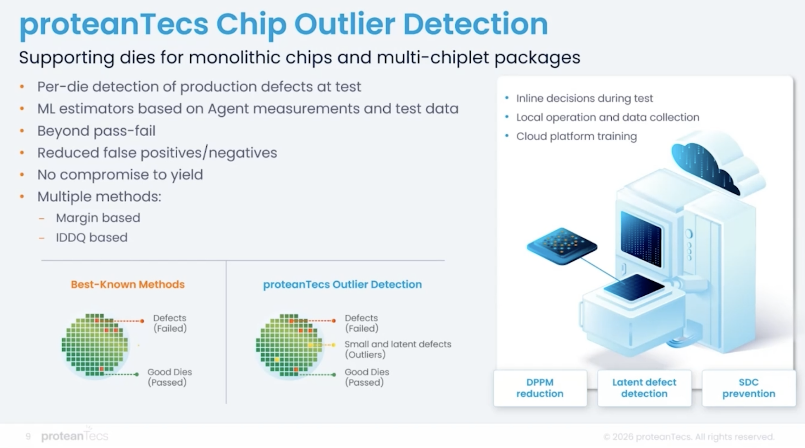
For manufacturers, this means pinpointing underlying defects before sinking extra money and time into packaging, final assembly, and downstream test cycles.
The payoff is massive for advanced packaging layouts. Catching these issues early during wafer sort enables smarter die selection, directly boosting final compound yields.
Unifying the Manufacturing Pipeline
Granular data becomes exponentially more useful when you bridge the gaps between different stages of the factory line. Advanced chip packages undergo a long journey: wafer sort, assembly, final test, and eventual system-level evaluations. Mapping and comparing how a device acts across these isolated milestones helps engineering teams track physical changes that occur post-packaging. This makes it far easier to isolate the actual root cause of a failure.
This data bridge creates an ongoing, iterative feedback loop:
Measure → Correlate → Identify → Improve
With this feedback loop in place, testing stops being a rigid gatekeeper. Instead, it evolves into active intelligence that optimizes both manufacturing precision and packaging choices.
Moving From Factory Gates to Lifetime Reliability
Deep visibility doesn’t lose its value the moment a packaged chip ships out the door. proteanTecs carries its tracking capabilities right into live, real-world operation. By monitoring timing margins and internal telemetry on deployed hardware, it keeps tabs on overall system health and notes performance drifts. Practical applications include real-time degradation tracking, predictive failure alerts, and remaining-useful-life computations.
This shift allows tech teams to stop simply reacting to sudden hardware crashes and start actively anticipating them. Having access to continuous field telemetry makes it easy to schedule proactive maintenance, swap out fading components, or alter system workloads before a critical failure happens.
Summary
Modern packaging layouts demand a complete rethink of traditional testing, quality control, and hardware reliability. Amkor’s deep packaging and testing expertise and proteanTecs’ internal silicon observability help to unlock a comprehensive approach for more reliable and longer lasting devices and systems, through:
- Early Vetting: Certify individual dies much earlier in the assembly cycle.
- Complex Testing: Confidently stress-test dense, multi-die systems.
- Granular Insight: Decode unique device behaviors using high-fidelity deep data.
- Smart Optimization: Fine-tune power and execution based on actual operational margins.
- Lifelong Tracking: Maintain visibility over devices throughout their entire field deployment.
For high-density packaging, this comprehensive approach directly drives higher compound yields and reduces factory scrap. It clears test-access hurdles, refines power distribution, and ensures long-term operational resilience.
As chiplet architectures become the definitive backbone for AI workloads and heavy computing, peering inside a package is becoming just as critical as the physical ability to manufacture it.
Eliminating blind spots does more than solve technical hurdles. Leveraging telemetry data coming off advanced hardware becomes a major competitive asset: actionable intelligence that delivers sharper manufacturing precision, optimized performance, and improved system stability.
To watch the webinar on-demand, visit here.
Also Read:
Podcast EP345: The Impact of the New proteanTecs PVT Plus Sensors with Nir Sever
proteanTecs at Chiplet Summit – Changing the Game for Health & Performance Monitoring of Chiplets
Intelligent Networks: Power, Reliability, and Maintenance in Telecom — Webinar Preview
Share this post via:



Comments
There are no comments yet.
You must register or log in to view/post comments.