In the rapidly evolving landscape of semiconductor technology, imec’s recent breakthroughs in wafer-to-wafer hybrid bonding and backside connectivity are paving the way for CMOS 2.0, a paradigm shift in chip design. Introduced in 2024, CMOS 2.0 addresses the limitations of traditional CMOS scaling by partitioning a system-on-chip (SoC) into specialized functional tiers. Each tier is optimized for specific needs—such as high-performance logic, dense memory, or power efficiency—through system-technology co-optimization (STCO). This approach moves beyond general-purpose platforms, enabling heterogeneous stacking within the SoC itself, similar to but more integrated than current 3D stacking of SRAM on processors.

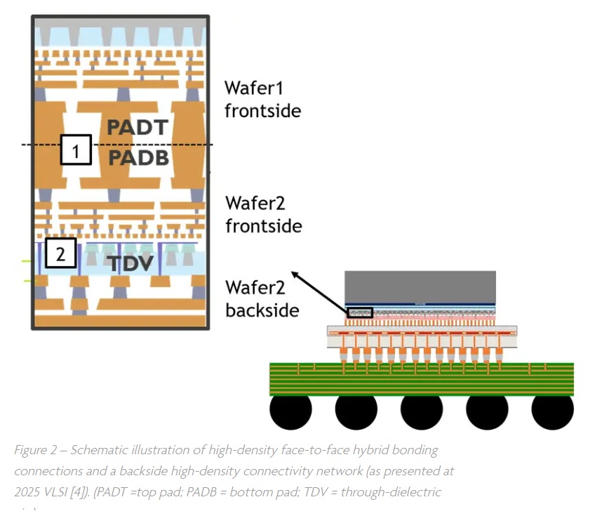
Central to CMOS 2.0 is the use of advanced 3D interconnects and backside power delivery networks (BSPDNs). These technologies allow for dense connections on both sides of the wafer, suspending active device layers between independent interconnect stacks. At the 2025 VLSI Symposium, imec demonstrated key milestones: wafer-to-wafer hybrid bonding at 250nm pitch and through-dielectric vias (TDVs) at 120nm pitch on the backside. These innovations provide the granularity needed for logic-on-logic or memory-on-logic stacking, overcoming bottlenecks in compute scaling for diverse applications like AI and mobile devices.
Wafer-to-wafer hybrid bonding stands out for its ability to achieve sub-micrometer pitches, offering high bandwidth and low-energy signal transmission. The process involves aligning and bonding two processed wafers at room temperature, followed by annealing for permanent Cu-to-Cu and dielectric bonds. Imec has refined this flow, achieving reliable 400nm pitch connections by 2023 using SiCN dielectrics for better strength and scalability. Pushing further, simulations revealed non-uniform bonding waves causing wafer deformation, impacting overlay accuracy. By applying pre-bond litho corrections, imec reached 300nm pitch with <25nm overlay error for 95% of dies. At VLSI 2025, they showcased 250nm pitch feasibility on a hexagonal pad grid, with high electrical yield in daisy chains, though full-wafer yield requires next-gen bonding tools.
Complementing frontside bonding, backside connectivity enables front-to-back links via nano-through-silicon vias (nTSVs) or direct contacting. For CMOS 2.0’s multi-tier stacks, this allows seamless integration of metals on both sides, with BSPDNs handling power from the backside to reduce IR drops and decongest frontside BEOL for signals. Imec’s VLSI 2025 demo featured barrier-less Mo-filled TDVs with 20nm bottom diameter at 120nm pitch, fabricated via a via-first approach in shallow-trench isolation. Extreme wafer thinning maintains low aspect ratios, while higher-order lithography corrections ensure 15nm overlay margins between TDVs and 55nm backside metals. This balances fine-pitch connections on both wafer sides, crucial for stacking multiple heterogeneous layers like logic, memory, and ESD protection.
BSPDNs further enhance CMOS 2.0 by relocating power distribution to the backside, allowing wider, less resistant interconnects. Imec’s 2019 pioneering work has evolved, with major foundries adopting it for advanced nodes. DTCO studies show PPAC gains in always-on designs, but VLSI 2025 extended this to switched-domain architectures—relevant for power-managed mobile SoCs. In a 2nm mobile processor design, BSPDN reduced IR drop by 122mV compared to frontside PDNs, enabling fewer power switches in a checkerboard pattern. This yielded 22% area savings, boosting performance and efficiency.
These advancements, supported by the NanoIC pilot line and EU funding, bring CMOS 2.0 from concept to viability. By enabling heterogeneity within SoCs, they offer scalable solutions for the semiconductor ecosystem, from fabless designers to system integrators. As pitches scale below 200nm, collaboration with tool suppliers will be key to overcoming overlay challenges. Ultimately, high-density front and backside connectivity heralds a new era of compute innovation, meeting demands for performance, power, and density in an increasingly diverse application space.
Also Read:
Exploring TSMC’s OIP Ecosystem Benefits
Synopsys Collaborates with TSMC to Enable Advanced 2D and 3D Design Solutions
Advancing Semiconductor Design: Intel’s Foveros 2.5D Packaging Technology
Share this post via:


Silicon Insurance: Why eFPGA is Cheaper Than a Respin — and Why It Matters in the Intel 18A Era