
At the recent IPSoC Conference in Silicon Valley, Aparna Tarde gave a talk on the importance of Next-Gen Interconnects to scale AI infrastructure. Aparna is a Sr. Technical Product Manager at Synopsys. A synthesis of the salient points from her talk follows.
The rapid advancement of artificial intelligence (AI) is fundamentally reshaping the requirements for data center infrastructure. Meta’s Llama 3, for instance, has 405 billion parameters and was trained on 16,000 Nvidia H100 GPUs using 15.6 trillion tokens, and took 70 days to train. These massive workloads demand not only immense compute resources but also unprecedented memory capacity and ultra-fast interconnects to sustain performance growth. To meet performance requirements, systems now rely heavily on efficient XPU-to-XPU communication. This demands high-bandwidth, low-latency, and energy-efficient interconnects capable of synchronizing large-scale compute clusters. Memory requirements are also becoming a challenge; for example, Llama 3.1 requires 854 GB of memory per model instance, while current GPUs like the Nvidia H200 offer only 141 GB, necessitating either memory scaling or advanced compression. To accommodate the growing needs of generative AI, data center architecture is being redefined. Traditional homogeneous resource pools are being disaggregated, while heterogeneous resources are aggregated to meet specific workload demands.

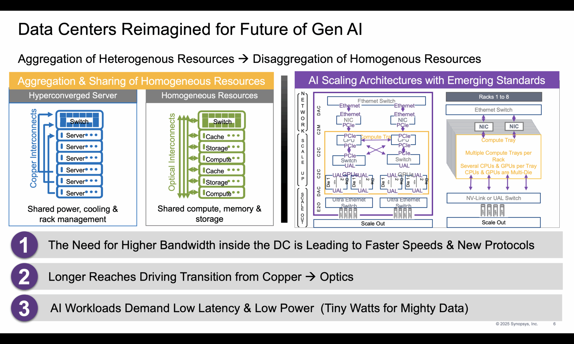
Higher bandwidth and new communication protocols are becoming essential, especially as longer communication reaches drive the shift from copper to optical links. AI workloads also impose strict requirements for low power consumption and latency.
The Role of Interfaces in AI and HPC SoCs
Efficient data movement within and between SoCs is becoming the cornerstone of AI scalability. At the same time, no single interface can address all AI workload requirements. Instead, a mix of standards is evolving to meet various demands: PCIe and CXL manage general-purpose and memory-centric workloads, UALink handles intra-node compute scaling, and Ultra Ethernet supports inter-node communication across large clusters. Together, these interfaces create a cohesive and open ecosystem, supplanting legacy proprietary networks and enabling more flexible and scalable infrastructure.

UALink: Scaling Up AI Performance
UALink is purpose-built to meet the demands of AI scale-up, offering a lightweight, high-bandwidth, open-standard interconnect optimized for XPU-to-XPU resource sharing and synchronization across up to 1,024 accelerators. Unlike PCIe 7.0, which lacks remote memory access, or CXL 3.x, which is slowed by complexity and adoption lag, UALink delivers streamlined performance without the overhead. By replacing proprietary networks and complementing existing standards, UALink provides the efficient, scalable backbone needed for next-gen AI systems.
Ultra Ethernet: Scaling Out AI Across the Data Center
As AI models grow more distributed, scale-out networking becomes critical. Ultra Ethernet is designed to meet this challenge, providing high bandwidth, multi-path routing, and low-latency communication between over 1 million endpoints. Unlike traditional Ethernet which struggles with configuration complexity, network congestion, and out-of-order delivery, Ultra Ethernet is optimized for simplicity and performance.
The Optical Shift: From Copper to Co-Packaged Optics
With data movement becoming a primary concern, the limitations of copper are more apparent than ever. Different interconnect mediums now serve distinct roles in the data center: PCB traces for intra-device links, copper for intra-rack communication, and optics for inter-rack distances. Co-Packaged Optics (CPO) is the next step in this evolution, integrating silicon and optical components within a single package to dramatically reduce power consumption and latency. Network switches bear the brunt of AI-related bandwidth scaling and are expected to be the early adopters of CPO.
Multi-Die Packaging: Enabling the Next Generation of AI SoCs
As single-die integration becomes insufficient for AI workloads, multi-die packaging technologies like 2.5D, 3D, and 3.5D are becoming mainstream. These techniques allow for metal-to-metal die connections that significantly reduce latency and power while increasing interconnect bandwidth. Though more complex and costly due to thermal modeling and bonding challenges, 3D stacking enables re-usable, scalable chiplet architectures. UCIe 2.0 is suitable for 2D and 2.5D integration, while UCIe-3D and 3DIO PHY support vertical die-to-die communication for 3D stacking. These approaches are essential for AI SoCs that require close cache-to-core coupling and high-speed D2D links.
Summary
AI infrastructure is undergoing a massive transformation driven by the need for more performance, efficiency, and scalability. Next-generation interconnects like UALink for scale-up and Ultra Ethernet for scale-out, combined with advanced optical links and multi-die packaging, form the foundation of tomorrow’s AI-powered data centers. Synopsys is enabling the buildup of next-gen AI infrastructure through its comprehensive and performance-optimized high-speed interface IP portfolio.

Learn more about Synopsys HPC IP Solutions
Also Read:
The Growing Importance of PVT Monitoring for Silicon Lifecycle Management
SNUG 2025: A Watershed Moment for EDA – Part 1
Share this post via:


Comments
There are no comments yet.
You must register or log in to view/post comments.