Establishing void-free fill of high aspect ratio TSVs, capped by a thin and uniform bulk layer optimized for removal by CMP, means fully optimizing each of a series of critical phases. As we will see in this 3-part series, the conditions governing outcomes for each phase vary greatly, and the complexity of interacting factors means that starting from scratch poses an empirical pursuit that is expensive and of long duration.
Robust and void-free filling of TSVs with copper progresses through six phases as laid out below:
- Feature wetting and wafer entry (previous article)
- Feature polarization
- Nucleation
- Fill propagation
- Accelerator ejection
- Bulk layer plating
- (Rinsing and drying, which we won’t cover in this series)
Fill Propagation
Ok, so, now that we’ve reached the third part of this 3 part series about TSV fill, we get to talk about the fill part of TSV fill.
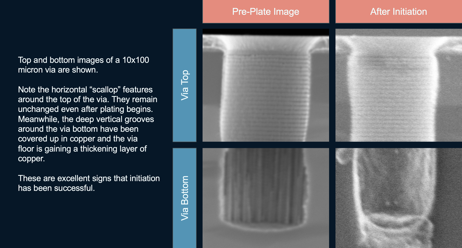
We wetted the features completely and our dwell step ensured that copper cations and accelerator molecules were able to gather in the bottom of the via. We initiated a potential on the system, driving a current that causes copper deposition to begin. If our via sidewall (especially low down) was characterized by significant roughness, we spiked that current density to get an even initiation of deposition. All that’s left is to let fill happen. Right?
Well, actually…yeah, largely that should be right. If we chose a good chemistry and we were careful in setting up polarization, confirming the initiation of bottom up fill through FIB/SEM inspection, the fill “should” go as planned.
Here’s where we see the delicate interaction of our organic additives at play. Suppressor, coating the upper wall of the via (as well as the entire surface of the wafer), increases the over-potential required to reduce the ions to metallic copper. Meanwhile, accelerator is adsorbed in concentration on the via floor and to some degree slightly up the via sidewall near the bottom. And, whereas the suppressor is busy making it harder for copper cations to be reduced, the accelerator is making it easier. Current is flowing, and, because in copper plating the plating efficiency approaches 100%, each electron that passes takes part in the reduction of copper ions and thus the formation of copper metal. Thus copper deposition is happening and it is happening in the one place where we made it easiest. The via bottom.
We have flipped the physics on its head.
A few interesting things happen now. As we shared, it takes real time for a cupric ion to diffuse to the via bottom. In the case of a 10X100 micron via, it may take as much as 5 seconds!! Thus the current density must be kept high enough to plate at a useful rate but low enough to avoid consuming the ions faster than they can diffuse down from the top of the via. Technically, it is possible to work a model to estimate this rate. Trial and error works too if you have access to wafers and inspection.
It’s time for a meaningful aside here.
First, it is not necessary to commit an entire wafer to each TSV fill test you run. TSV wafers can be cleaved into pieces (we typically call them coupons) and fill can be optimized by running the tests on the individual coupons. This saves a LOT of wafers. A coupon 4cm X 4cm would suffice. At this size (depending on feature layouts) you could possibly cleave 7 or 8 coupons from a 150mm TSV wafer and as many as 18 from a 200mm. That’s a lot more tests!
There are some tricks to successfully mounting and plating coupons and the supplies that make it easy are readily found in online stores like Amazon. If interested to learn more, hit us up at info@techsovereignpartners.com.
Once you’ve gotten fill optimized on coupons, transferring the recipe to a full wafer is all about scaling the current to maintain the current density (pay close attention to the actual open area of the wafer); and making sure deposition rates are equal across the wafer diameter. Cross-wafer uniformity establishment is a topic all on its own not only applicable in TSV fill but in plating generally; we won’t cover in today’s discussion.
That’s it for our aside, back to propagation of fill. Superconformal deposition, i.e. fill, is happening. The sidewall copper of the via is staying thin but the bottom is getting thicker. If it is not, and instead deposition is conformal (happening on both sidewalls and bottom) or sub-conformal (happening really only on the walls and not the bottom), then there are two likely root cause possibilities (and both may be at play).
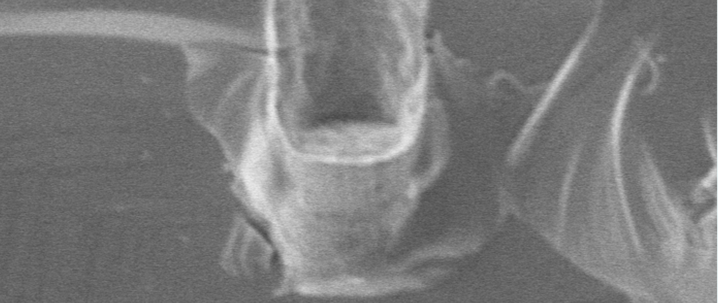
Before we explore root causes, let’s talk about how one determines whether super conformal fill is happening in the first place. As we said, and you likely already know, TSV fill can be a long process step, even an hour or more. FIB/SEM is a quite indispensable means of inspection for determining the performance of fill. But even the FIB cut can take a long, long time and FIB time is expensive. For these reasons and more, we recommend that, when working to optimize fill, you do not attempt to fill the entire via. Aim, instead, for a 1/4 or 1/3 fill, i.e. a partial fill. This makes each test go much faster and the FIB cuts faster too. More importantly, though, it shows you with clarity whether superconformal fill is happening or not. As we said in the previous article, if you did not get polarization right in the beginning, no recipe adjustment is going to fix it. Continue optimizing through imaging of partially filled vias until you confirm that copper growth is minimal or undetectable on the upper sidewalls and robust on the bottom.

Meanwhile, back to root causes when this is not evident. As stated, we likely have two. They are:
- The current setpoint is not optimal.
- The additive ratios are not optimal.
First, current setpoint. Here’s a dirty little secret about “setting current”. You are actually setting potential (voltage). The cell (electrolyte, hardware of the reactor and the wafer itself) then determine a current based on that potential. Ideally, the power supply you use does allow a current setpoint but what it is actually doing is aiming for a potential that it expects will produce your target current, and adjusting based on ammeter output to settle on target. But there’s more, it isn’t really current you are after; it’s current density. And now, the geometry, size and count of vias plays a direct part in converting that current into a current density. Your chemistry vendor ideally has provided you with a target current density, from which you can calculate a target current based on the dimensions and number of vias on your wafer. If no target current density is provided, you’ve bought a ticket on the DOE express and you have some work to do.
Second is the additive ratios. Really, your chemistry vendor has almost certainly provided you with target additive ratios based on their own studies. You are certainly welcome to perform your early optimization tests by varying these ratios, however we would recommend trusting those ratios at the start. Crafting and executing a DOE around just current setpoints will be time consuming already. Adding a second parameter will of course greatly expand the test set, but including additive ratio tests also means dumping and re-pouring the bath again and again. Again, the chemistry vendor has likely determined an optimal ratio of additives. If they have not, or you have a via of highly non-standard dimensions, you may not be able to escape additive ratio testing.
So, through attentive preparation and testing, you established good bottom up fill, as verified by FIB/SEM imaging. In other words, the floor of the via is rising. This is exciting and you deserve a drink. But don’t forget, you were only doing partial fills so you are actually not done at all.
There are a few effects of this rising floor phenomenon. First, accelerator, generally speaking, does not get integrated into the plated copper, meaning that it continues to “ride the floor” as the via fills. Any accelerator adsorbed to the lower sidewalls is now getting swept up and added to the accelerator on the floor, increasing the concentration further. Incidentally, sidewall suppressor is getting displaced along the way. Acceleration is accelerating, in a sense. Fill may be moving faster in terms of vertical growth. That’s nice for throughput.
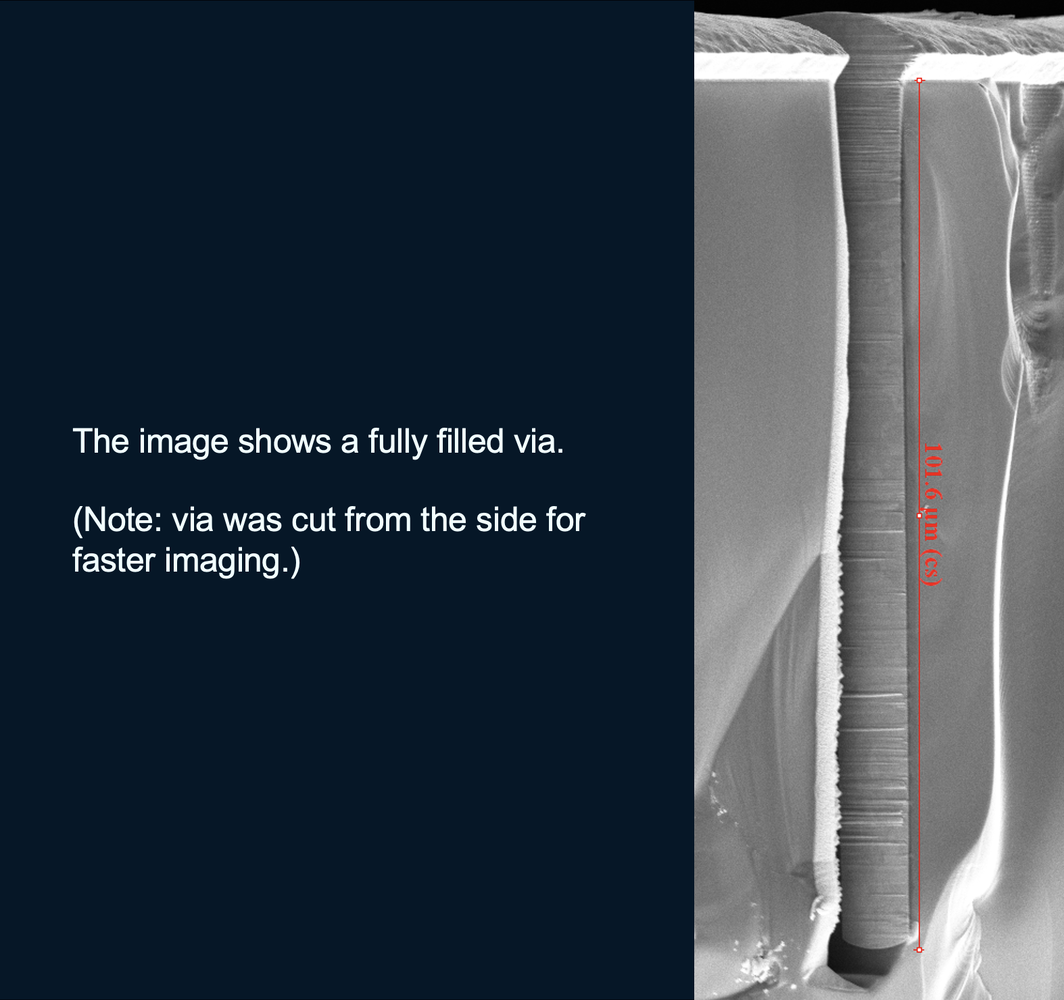
The other thing that’s happening is that the long, long time it was taking for copper ions to get down to the via bottom is getting shorter and shorter because the via is getting shorter and shorter. Your high aspect ratio via is becoming a moderate to low aspect ratio via. So this means, if throughput matters to you, you can make edit the recipe such that it starts as a “high aspect ratio via” recipe and modulates to a “moderate” and finally “low aspect ratio via” recipe. You can run what we’d commonly call a stair-step recipe. Which means that, at the start of fill, we use a relatively low current that maintains good fill (based on the current density recommended by your chemistry vendor and your via dimension calculations), then at some point later, when the via is shorter (for a 10X100micron via maybe a quarter shorter) the current can be stepped up higher. And then again later, and then again. Don’t get me wrong, fill “should” progress fine without stepping up the current. But faster is better. A stair-step recipe well constructed should fill a 10X100 micron via in under an hour. Without the stair-step, this fill time can be much, much longer.

Accelerator Ejection
Ok the via floor is approaching the top! This is great news. Unless you forgot about the brakes. Remember, we basically super charged the via floor with spicy, spicy accelerator molecules. They’re doing their job and that via floor is rushing up to the top of the hole. We’d like it to conveniently stop, pretty please, immediately at the top. But will it? In fact, it will not without proper attention and mounds will form above the vias, creating major problems in CMP, typically leaving un-polished copper bumps over every via. This is of course a no go for subsequent steps in the integration.
So what to do about it. The easy button is to, well, not get cheap when selecting a TSV chemistry. Chemical displacement is your friend when it comes to accelerator ejection and the avoidance of forming copper humps above your vias. A carefully and properly formulated leveler polymer is key here. In advanced TSV chemistries, the leveler magically ejects the accelerator as it reaches the top of the via hole. Easy.
Ok, what if your TSV chemistry works fine but doesn’t do the magic ejection thing? There is still a solution for you. You can force the ejection of ALL additives from all surfaces of what is now essentially a flat, copper coated wafer with no holes in it. Doing so requires two things: the right timing and the right power supply. First timing: You need to know when, in your recipe, the copper has reached the top of the hole. Again this can be done in coupon testing for recipe optimization. At the point when copper has reached the top, you can introduce a reverse pulse of the power supply in your recipe. Hence the second point, you would need the right power supply. A supply that is capable to pulse is very valuable in copper plating. A power supply that can pulse with a forward potential (one that deposits copper onto the wafer) and can also pulse with a reverse potential (one that removes copper from a wafer) provides even more flexibility.
Introducing a brief pulse in reverse will cause all additives to eject from the entire wafer surface. The step can be very short because the ejection is nearly instantaneous. We would recommend a short step, perhaps 50 milliseconds, and for simplicity we would recommend using the initial current at the beginning of your fill (not the high current nucleation step). Now you’ll return to forward potential for the bulk layer plating and additive adsorption will be what it will be; you don’t really care because the entire surface will see the same species adsorption now that the advantages associated with tall via holes is eliminated.

Bulk Layer Plating
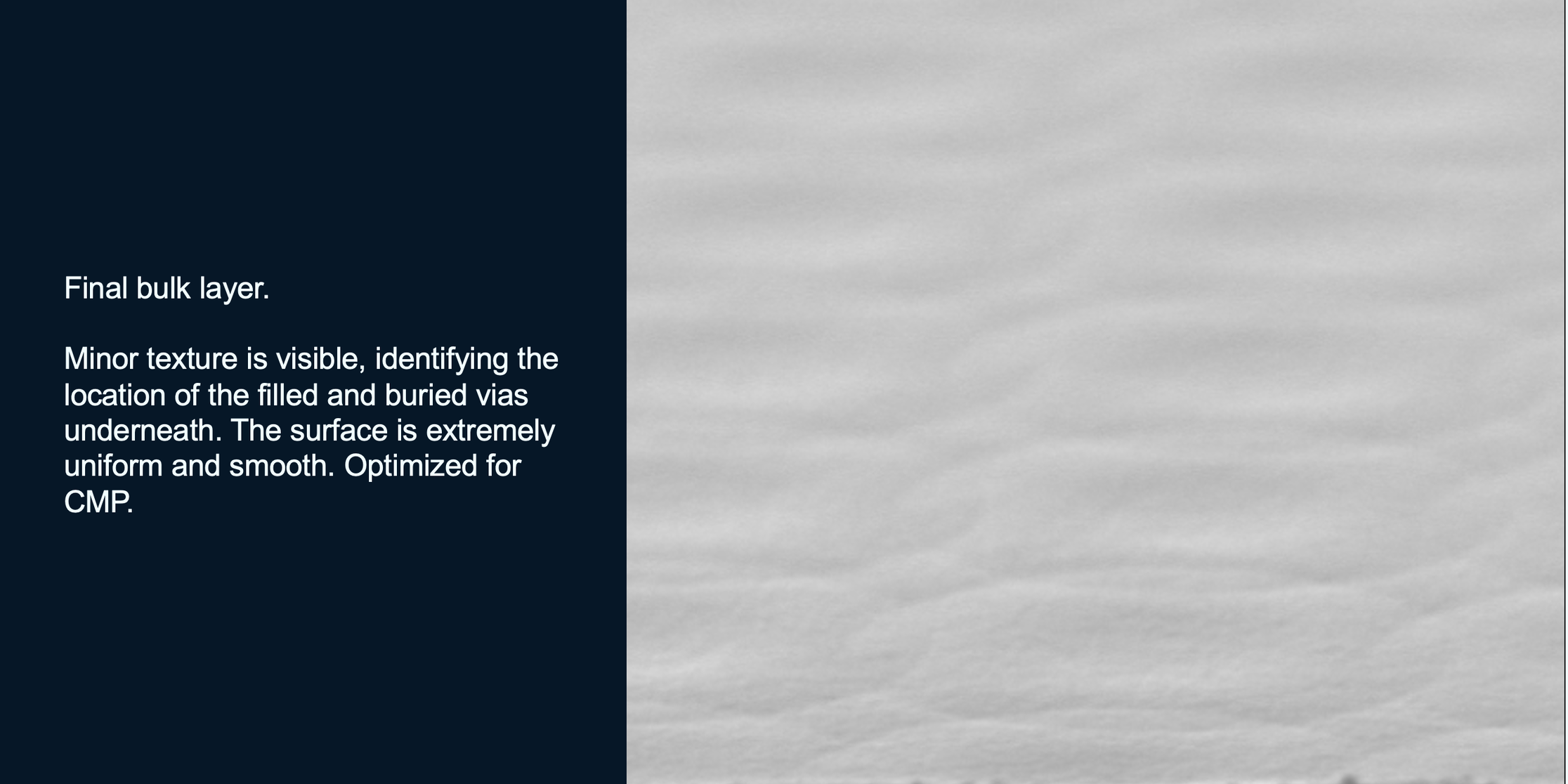
Vias are filled. There were no voids. Well, you hope there’s no voids. I’m not sure you really checked every via. Anyway, you also ejected all that accelerator you worked so hard to adsorb (sigh). And now you need a layer of sacrificial copper on top of it all so that the CMP folk can polish it back to leave a perfectly flat hybrid surface of silicon perforated by neat little copper circles belying tall and slender, buried pillars of pristine copper.
Well, generally speaking, you can crank that power supply up now. As long as you’ve established good cross-wafer plating rate uniformity, you can go as fast as the chemistry can keep up with. 40 amps on a 300mm wafer is legitimate with most TSV chemistries. We can do the math. That’s about 18 amp on a 200mm wafer and 10 amp on a 150mm wafer.
So, you’re good at this and that film is very uniform. The question is, how thick do you make it? The answer is, I don’t really know for sure, sorry. For that you’ll have to talk to your CMP people. CMP, of course, takes advantage of insitu uniformity tracking and can make closed loop adjustments to maintain uniform removal. Exactly how quickly a uniform polish can be established depends on the optimization and the capabilities of that tool set. Obviously, CMP is one of the more expensive unit processes in the fab and financial controllers and fab managers will be interested to keep those costs as low as is practical. No, they’ll probably want costs lower than practical but that’s why they hired you. So, this means keeping that film as thin as possible, both from the plating perspective (maintaining uniformity) and the CMP perspective (uniform polish). That sounds like more DOE work. I hope you’ve looked up what “DOE” means by now.
If you have questions about TSV fill or some of the sub-topics raised in these articles, do reach out at info@techsovereignpartners.com
Also Read:
Mastering Copper TSV Fill Part 2 of 3
Mastering Copper TSV Fill Part 1 of 3
Share this post via:


Intel, Musk, and the Tweet That Launched a 1000 Ships on a Becalmed Sea