You are currently viewing SemiWiki as a guest which gives you limited access to the site. To view blog comments and experience other SemiWiki features you must be a registered member. Registration is fast, simple, and absolutely free so please,
join our community today!
Establishing void-free fill of high aspect ratio TSVs, capped by a thin and uniform bulk layer optimized for removal by CMP, means fully optimizing each of a series of critical phases. As we will see in this 3-part series, the conditions governing outcomes for each phase vary greatly, and the complexity of interacting factors means… Read More
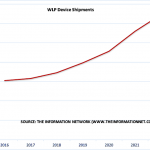
Advanced IC packaging, such as fan-out WLP (Wafer Level Packaging) and 2.5D TSV (Through Silicon Via) will drive the packaging equipment market, particularly lithography. This will help specific equipment manufacturers in 2019, since the WFE (Wafer Front End) market will drop 17%. But the Back-End lithography market, led … Read More