You are currently viewing SemiWiki as a guest which gives you limited access to the site. To view blog comments and experience other SemiWiki features you must be a registered member. Registration is fast, simple, and absolutely free so please,
join our community today!
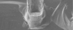
Establishing void-free fill of high aspect ratio TSVs, capped by a thin and uniform bulk layer optimized for removal by CMP, means fully optimizing each of a series of critical phases. As we will see in this 3-part series, the conditions governing outcomes for each phase vary greatly, and the complexity of interacting factors means… Read More
For IC designers creating full-custom or AMS designs there are plenty of challenges to getting designs done right on the first spin of silicon. Let me give you a sneak peek into what’s being discussed at the EDA Tech Forum in Santa Clara, CA on March 10th that will be of special interest to you:
3D TSV (Through Silicon Vias) are… Read More