So DAC is over and you are no longer thinking about the features and benefits of new tools or even the tools that you already own. But once you have lots of tools then you need to worry about how to use them efficiently.
But here are three things that you need to worry about to get the most out of your EDA investment:
- how do you measure the actual license usage?
- how do you build best of breed flows to encapsulate the tools you have invested in?
- how do you maximize the use of the licenses you have invested in?
This is increasingly important since both the scale of the hardware infrastructure (server farms, perhaps with a wide range of different machines) and the scale of the jobs themselves (huge number of runs) are enormous.
Runtime Design Automation (RTDA) has three tools that address the three problems above and which scale to the size of the infrastructure and the jobs.
LicenseMonitor is a tool for gathering data on license usage and displaying it in useful intuitive ways. It operates with most license managers such as FlexLM.
FlowTracer captures all the details of a flow and so allows best-in-class flows to be created and deployed across an organization.
NetworkComputer is the fastest available commercial job scheduler. It interfaces with license managers to make efficient use of the licenses and can even statistically over-schedule. It can share licenses across an organization based on demand and policies, and use pre-emption to ensure licenses are allocated to important jobs (such as designs nearing tapeout).
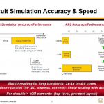
As an example, RTDA told me about a typical timing run that a customer would make. It is a block flow of timing runs with 45 timing corners multiplied by plain/noise/interface-logic-models making 135 jobs in parallel (and 144 for the full-chip runs). This is completely distributed across a farm taking into account availability of both servers and licenses.
Download the LicenseMonitor datasheet.
Download the FlowTracer datasheet.
Download the NetworkComputer datasheet.