IC device physics uncovers limits to reliable operation, so IC designers are learning to first identify and then fix reliability issues prior to tape-out. Here’ s a list of reliability issues to keep you awake at night:
Continue reading “IC Reliability and Prevention During Design with EDA Tools”
Next Generation Transistors
We have all heard that planar transistors have run out of steam. There are two ways forward. The one that has garnered all the attention is Intel’s trigate which is their name for FinFET. The other is using thin film SoI which ST is doing. TSMC and Global seem to be going the FinFET way too, although at a more leisurely pace. But why are planar transistors running out of steam? And why are these the two promising ways forward? Dr Chenmin Hu, the inventor of the FinFET first described in a 1999 paper (pdf), gave us all a tutorial. It was fascinating. I thought that most of the power of the FinFET came because the gate wraps around the channel on three sides and three is better than one. But that is not the real story.
A planar MOS transistor theoretically should have a performance of 63mV/decade (which comes from the distribution of electron potentials trying to get out of the source through the gate). But this assumes that all of the channel region is fully controlled by the gate. The deeper down into the channel you go, and thus the farther from the gate, the less it is controlled. In practice, this means that current can slink through even when the gate is “off” which is why leakage power has become such a big problem. In effect the transistor has become a resistor and cannot control the current.
Solution #1: reduce the oxide thickness. This is what we have done for decades. But this still cannot control the channel far from the gate since the voltages have come down too. So the solution is to ensure that there is no silicon far from the gate. That way the whole channel will be well-controlled by the gate.
There are two ways to ensure that there is no silicon far from the gate. One is the FinFET. Build a fin (the name comes from being like a fin on a fish) for the channel and then wrap the gate over the top of the fin. The key parameter is to make the fin thinner than the gate width. That way the whole channel is completely controlled by the gate since everywhere in the channel is close enough to the gate. Working FinFETs have been built at 5nm and 3nm (using e-beam so not economic for mass production, but the technology works at those dimensions).
There have been two big improvements to the FinFET since the original paper in 1999. Firstly TSMC worked out how to put thin oxide on top of the fin (the original fin was effectively 2-sided). Intel is the company first making use of this but, as Dr Hu pointed out, TSMC can take credit. Ironic. The second is in 2003 Samsung worked out how to build FinFETs on bulk substrate (they were SoI in the original paper).
Since FinFET and planar transistors use many of the same manufacturing steps and are completely compatible, the low risk approach would be to mix them and have both available on the same chip. So apparently it was a surprise when Intel decided not to do this and have a FinFET-only process at 22nm.
The second way to make sure that there is no silicon far from the gate is to go away from a bulk silicon process and instead use an insulator, put a thin layer of silicon on it, and then build planar transistors in the normal way. There is no silicon far from the gate because if you go that deep it is no longer silicon, you are into the insulator layer (where obviously no current can flow).
This is the approach ST is taking and was explained in a lot more detail by Joël Hartman of ST. They believe that it has the best speed/power performance. The gate region is fully depleted so this technology is known as FD-SOI (not quite as catchy as FinFET or even Tri-gate). ST reckon that due to lithographic reasons 28nm will be a golden-node with a long lifetime. They currently have planar 28nm and they are introducing FD-SOI first at 28nm as a sort of second generation, before introducing it at 20nm. They also feel that without some unanticipated breakthrough neither EUV nor double/triple patterning will be economical at 14nm and they will probably have a process in the gap that for now they are calling 16nm although it might be anwyhere between 14 and 20nm (with a less complex process).
So there you are: planar transistors are at the end of their life because too much silicon is far from the gate and so not turned off by the gate. So make sure no silicon is far from gate. Either build a thin fin and wrap the gate around it, or switch from bulk silicon to a thin film of silicon on an insulator. Hence the future is FinFET and/or FD-SOI and we’ll see how this plays out.
Keeping Moore’s Law Alive
At the GSA silicon summit yesterday the first keynote was by Subramanian Iyer of IBM on Keeping Moore’s Law Alive. He started off by asking the question “Is Moore’s Law in trouble?” and answered with an equivocal “maybe.”
Like some of the other speakers during the day, he pointed out that 28nm will be a long-lived process, since the move to 20nm is not really that compelling (for instance, despite Intel’s $12B investment, comparing Sandy Bridge and Ivy Bridge there is a 4% reduction in power for roughly the same performance).
As most of us know, we lack a viable lithography that is truly cost-effective for 20nm and below. We have a workable technology in double patterning, but the cost of a mask set, the cost of the extra manufacturing steps and the impact on cycle time are enough to knock us off the true Moore’s law trajectory which is not a technology law but an economic one. Namely, that at each process generation the transistors are about half the cost compared to the previous generation. People have successfully created 3nm FinFET transistors using e-beam but that isn’t close to scaling to volume manufacturing.
As Roawen Chen pointed out at the start of the later panel session, sub 20nm we are looking at some steep hills:
- $200M per thousand wafer starts per month capacity
- $10B for a realistic capacity fab
- EUV or double/triple patterning
- $7M for a mask set
- $100M per SoC design costs
- Fab cycle time (tapeout to first silicon) of 6 months (one year with a single respin)
Subu focused on what he called “orthogonal scaling” meaning scaling other than what we normally call scaling, namely lithographic scaling. And, as he pointed out, IBM is an IDM and so not everything he says is necessarily good for the foundry model.
The first aspect of orthogonal scaling that IBM is using is embedded DRAM. Everyone “knows” that SRAM is much faster than DRAM and this is true. But as memories get larger, the flight time of the address and data is the dominant delay and DRAM starts to perform better since it is smaller (so shorter flights). Plus, obviously, the overall chip is smaller (or you can put more memory).
A second benefit of embedded DRAM is that you can build deep trench capacitors which are 25X more effective per unit area than other capacitors and so can be used heavily for power supply decoupling. This alone gives a 5-10% performance increase, which is an appreciable fraction of a process generation.
Power is the big constraint. But 70-80% of power in a big system is communicating between chips. The processor dissipates about 30% of the power, I/O dissipates about 20% and memory about 30%, but half of the memory power is really I/O. 3D chips give a huge advantage. The distances in the Z direction are much smaller than in the XY direction and you can have much higher bandwidth since you can have thousands of connections and the power dissipation is a lot less than multiplexing a few pins at very high clock rates.
So the reality of Moore’s Law. We have marginally economic lithography at 20nm, unclear after that. EUV is still completely unproven and might not work. Double and triple patterning are expensive (and create their own set of issues since the multiple patterns are not self-aligning leading to greater variation in side-wall capacitance, for example). Ebeam write speed is orders of magnitude too slow. But orthogonal approaches can, perhaps, substitute in at least some cases.
Introduction to FinFET technology Part II
The previous post in this series provided an overview of FinFET devices. This article will briefly cover FinFET fabrication.
The major process steps in fabricating silicon fins are shown in Figures 1 through 3. The step that defines the fin thickness uses Sidewall Image Transfer (SIT). Low-pressure chemical vapor (isotropic) deposition provides a unique dielectric profile on the sidewalls of the sacrificial patterned line. A subsequent (anisotropic) etch of the dielectric retains the sidewall material (Figure 1). Reactive ion etching of the sacrificial line and the exposed substrate results in silicon pedestals (Figure 2). Deposition of a dielectric to completely fill the volume between pedestals is followed by a controlled etch-back to expose the fins (Figure 3).
Figure 1. Cross-section of sidewalls on sacrificial lines after CVD etch.
Figure 2. Cross-section of silicon pedestals after RIE etch, using Sidewall Image Transfer.
Figure 3. Cross-section of silicon fins after oxide deposition and etch-back, and gate deposition.
Low-pressure dielectric deposition to create sidewalls on a polysilicon line is a well-known technique – it is commonly used to separate (deep) source/drain implant areas from the planar FET transistor channel. FinFET fabrication extends this technique to pattern definition for silicon fin etching.
There is no photolithography step associated with SIT, just the patterning of the sacrificial lines. As a result, the fin thickness can be smaller than the photolithographic minimum dimensions. The fin thickness is defined by well-controlled dielectric deposition and etching steps rather than photoresist patterning, reducing the manufacturing variation. However, there is variation in fin height, resulting from (local) variations in the etch-back rate of dielectric removal. (For FinFET’s on an SOI substrate, the fin height is defined by the silicon layer thickness, with a ‘natural’ silicon etch-stop at the insulator interface in contrast to the timed-etch fin height for bulk substrate pedestals.)
There are several characteristics to note about SIT technology. Nominally, fins come in pairs from the two sidewalls of the sacrificial line. Adding fins in parallel to increase drive current typically involves adding a pair of fins: delta_w = (2*(2*h_fin + t_fin)).
To “cut” fins, a masked silicon etching step is required. There are two considerations for cutting fins. The first involves breaking long fins into individual pairs. The other is to create an isolated fin, by removing its SIT-generated neighbor. Critical circuits that require high density and/or different device sizing ratios may justify the need for isolated fin patterning – e.g., SRAM bit cells. Compared to cutting, isolated fin patterning may involve different design rules and separate (critical) lithography steps, and thus additional costs.
Additional process steps are required to introduce impurities of the appropriate type below the fin to provide a punchthrough stop (PTS), ensuring there is no direct current path between drain and source that is not electrostatically controlled by the gate input.
The dielectric between pedestals that remains after etch-back serves as the field oxide, as denoted in Figure 3. The gate material traversing between parallel fins is well-separated from the substrate, minimizing the Cgx parasitic capacitance.
The uniformity and control of the final fin dimensions are important process characteristics, for both the fin thickness and fin corner profiles. (The profile of the pedestal below the fin is less critical, and may be quite tapered, as shown in Figure 3.) Tolerances in the fin thickness arise from variations in the vertical, anisotropic SIT silicon etch. The fin thickness at the bottom is also dependent upon the uniformity of the etch-back – the goal is to minimize any dielectric “foot” remaining at the bottom of the fin.
As will be discussed in the next series installment, variations in t_fin have significant impact upon the transistor model. The top corner profiles also have an impact upon the transistor behavior, as the electric fields from the gate to the silicon fin are concentrated in this region, originating from both the sidewall and top gate materials.
Gate patterning follows conventional photolithographic steps, although the recent introduction of metal gate materials has certainly added to the complexity, especially as the gate must now traverse conformally over parallel fins. As with a planar FET technology, the gate length is the ‘critical dimension’ that is typically quoted as the basis for the process node – e.g., 20nm.
In contrast to planar FET technologies, providing multiple FinFET threshold voltage (Vt) offerings requires significant additional process engineering. The threshold of any FET is a function of the workfunction potential differences between the gate, dielectric, and silicon substrate interfaces. In planar FET’s, multiple Vt offerings are readily provided by shallow (masked) impurity implants into the substrate prior to gate deposition, adjusting the workfunction potential between dielectric and channel. However, the variation in the (very small) dosage of impurities introduced in the planar channel results in significant Vt variation, due to ‘random dopant fluctuation’ (RDF).
With FinFET’s, there is ongoing process development to provide different metal gate compositions (and thus, metal-to-dielectric workfunctions) as the preferred method for Vt adjust. The advantage of using multiple gate metals will be to reduce the RDF source of Vt variation substantially, as compared to implanting a (very, very small) impurity dosage into the fin volume. The disadvantage is the additional process complexity and cost of providing multiple metal gate compositions.
Another key FinFET process technology development is the fabrication of the source/drain regions. As was mentioned in the first series installment, the silicon fin is effectively undoped. Although advantageous for the device characteristics, the undoped fin results in high series resistance outside the transistor channel, which would otherwise negate the drive current benefits of the FinFET topology.
To reduce the Rs and Rd parasitics, a spacer oxide is deposited on the FinFET gate sidewalls, in the same manner as sidewalls were patterned earlier for SIT fin etching. To increase the volume of the source/drain, a ‘silicon epitaxy growth’ (SEG) step is used. The exposed S/D regions of the original fin serve as the “seed” for epitaxial growth, separated from the FinFET gate by the sidewall spacer. Figure 4 shows the source/drain cross-section after the SEG step.
Figure 4. Cross section of source/drain region, after epitaxial growth. Original fin is in blue — note the faceted growth volume. The current density in the S/D past the device channel to the silicide top is very non-uniform. From Kawasaki, et al, IEDM 2009, p. 289-292.
The incorporation of impurities of the appropriate type (for nFET or pFET) during epitaxial growth reduces the S/D resistivity to a more tolerable level. The resistivity is further reduced by silicidation of the top of the S/D region. In the case of pFET’s, the incorporation of a small % of Ge during this epitaxy step transfers silicon crystal stress to the channel, increasing hole carrier mobility significantly.
Raised S/D epitaxy has been used to reduce Rs/Rd for planar FET’s, as well. However, there are a couple of interesting characteristics to FinFET S/D process engineering, due to the nature of the exposed fin S/D nodes, compared to a planar surface.
The epitaxial growth from the exposed crystalline surface of the silicon fin results in a “faceted” volume for the S/D regions. Depending upon the fin spacing and the amount of epitaxial growth, the S/D regions of parallel fins could remain isolated, or could potentially “merge” into a continuous volume. The topography of the top surface for subsequent metallization coverage is very uneven. The current distribution in the S/D nodes outside the channel (and thus, the effective Rs and Rd) is quite complex.
FinFET’s could be fabricated with either a HKMG ‘gate-first’ or a ‘gate-last’ process, although gate-last is likely to be the prevalent option. In a gate-last sequence, a dummy polysilicon gate is initially patterned and used for S/D formation, then the gate is removed and the replacement metal gate composition is patterned.
FinFET’s also require a unique process step after gate patterning and S/D node formation, to suitably fill the three-dimensional “grid” of parallel fins and series gates with a robust (low K) dielectric material.
Contacts to the S/D (and gate) will leverage the local interconnect metallization layer that has recently been added for planar 20nm technologies.
The next installment of this series will discuss some of the unique FinFET transistor modeling requirements.
Also read: Introduction to FinFET Technology Part III
Kadenz Leben: CDNLive! EMEA
If you are in Europe then the CDNLive! EMEA user conference is in Munich at the Dolce Hotel from May 14th to 16th. Like last month’s CDNLive! in Cadence’s hometown San Jose, the conference focuses on sharing fresh ideas and best practices for all aspects of semiconductor design from embedded software down to bare silicon.
The conference will start on Tuesday May 15th with a keynote presentation by Lip-Bu Tan (Cadence’s CEO, but you knew that). This will be followed by an industry keynote from Imec’s CEO Luc van den Hove.
After that are more than 60 technical sessions, tutorials and demos. There will also be an expo where companies such as Globalfoundries, Samsung and TSMC will exhibit.
Further, the Cadence Academic Network will host an academic track providing a forum to present outstanding work in education and research from groups or universities. The Network was launched in 2007 to promote the proliferation of leading-edge technologies and methodologies at universities renowned for their engineering and design excellence.
The conference fee is €120 + VAT (total €142.80)
The conference hotel is:Dolce Hotel
Andreas-Danzer-Weg 1,
85716 Unterschleißheim,
Germany
To register for CDNLive! EMEA go here.
Intel’s Ivy Bridge Mopping Up Campaign
In every Intel product announcement and PR event, there are hours of behind the scenes meetings to discuss what they should introduce, what are the messages and what are the effects on the marketplace to maximize the impact of the moment. The Ivy Bridge product release speaks volumes of what they want to accomplish over the coming year. If I could summarize, they are primarily, as I mentioned in a recent blog, in a mopping up operation with respect to nVidia and AMD, however with a different twist. And second, Intel is ramping 22nm at a very rapid pace, which means Ivy Bridge ultrabooks and cheap 32nm Medfields are on their way.
When Ivy Bridge was launched, I expected a heavy dose of mobile i5 and i7 processors and a couple ULV parts as well. We didn’t get that. What we got instead was a broad offering of i5 and i7 Desktop processors and high end i7 mobile parts with high TDP (Thermal Design Point) geared towards 7lb notebooks. I believe Intel shifted their mix in the last couple months in order to take advantage of the shortfall of 28nm graphics chips that were expected to be available from nVidia and AMD. When the enemy is having troubles, then it is time to run right over them. You see, Intel believes that they may be able to prove to the world, especially corporate customers that external graphics is unnecessary for anyone except teenage gamers and why wait for the parts from nVidia and AMD.
In a couple weeks, Intel will have their annual Analyst Meeting. I expect that they will highlight Ivy Bridge and the future Haswell architecture in terms of overall performance, low power and especially graphics capabilities. The overriding theme is that Intel has found a way to beat AMD and nVidia with a combination of leading edge process and a superior architecture. Rumors are that Haswell will include a new graphics memory architecture in order to improve performance. I am not a graphics expert, but I do know improved memory systems are always a performance kicker.
But back to the short term, which is what I find so interesting. Product cycles are short and Intel knows that shipping a bunch of Ivy Bridge PCs into the market without external graphics for the next 3-6 months can put a dent in nVidia and AMDs revenue and earnings, which will hurt their ability to compete long term. I expect both to recover somewhat by Fall, but by then Intel will shift its focus to ultrabooks and mobiles making a stronger argument that the Ivy Bridge graphics is sufficient and the best solution for maximizing battery life in mobiles. At that point they should start to cannibalize from the mobile side of AMD and nVidia’s business. Both companies could be looking at reduced revenues for the remainder of the year.
Bottom line to these tactical strategies is that Intel seeks to generate additional revenue off the backs of AMD and nVidia. In the near term it should come from the desktop side and then later in the Summer and Fall from the Mobile side. There is $10B of combined nVidia and AMD revenue for Intel to gold mine, which is much more than what they could accrue by pushing their Smartphone strategy ahead of their PC mopping up operation. A weakened AMD and nVidia will have a hard time fighting off the next stage, which is the Haswell launch in 1H 2013 and the coming 22nm Atom processors for smartphones and tablets.
FULL DISCLOSURE: I am long AAPL, INTC, ALTR and QCOM
Do you need more machines? Licenses? How can you find out?
Do you need more servers? Do you need more licenses? If you are kicking off a verification run of 10,000 jobs on 1,000 server cores then you are short of 9000 cores and 9000 licenses, but you’d be insane to rush out with a purchase order just on that basis. Maybe verification isn’t even on the critical path for your design, in which case you may be better pulling some of those cores and re-allocating them to place and route or DRC. Or perhaps another 50 machines and another 50 licenses would make a huge difference to the overall schedule for your chip. How would you know?
When companies had a few machines, not shared corporate wide, and a comparatively small number of licenses, these questions were not too hard to get one’s head around, and even if you were out by a few percent the financial impact of an error would not be large. Now that companies have huge server farms and datacenters containing tens if not hundreds of thousands of servers, these are difficult questions to answer. And the stakes are higher. Computers are commoditized and cheap, but not when you are considering them in blocks of a thousand. A thousand simulation licenses is real money too, never mind a thousand place & route licenses.
The first problem is that you don’t necessarily have great data on what your current usage is of your EDA licenses. RunTime Design Automation’s LicenseMonitor is specifically designed for this first task, getting a grip on what is really going on. It pulls down data from the license servers used by your EDA software and can display it graphically, produce reports and generally give you insight into whether licenses are sitting unused and where you are tight and licenses are being denied or holding up jobs.
The second challenge is to decide what would happen if you had more resources (or, less likely, fewer, such as when cutting outdated servers from the mix). More servers. More software licenses. This is where RunTime’s second tool WorkloadAnalyzer comes into play. It can take a historical workload and simulate how it would behave under various configurations (obviously without needing to actually run all the jobs). Using a tool like this on a regular basis allows tuning of hardware and software resources.
And it is invaluable coming up to the time to re-negotiate licenses with your EDA vendors, allowing you to know what you need and to see where various financial tradeoffs will leave you.
In the past this would all have been done by intuition but this approach is much more scientific. The true power of the tool lies in its Sensitivity Analysis Directed Optimization capability. This tells you which licenses or machines to purchase (or cut), and by how much, given a specific budget, such that doing so would produce the greatest decrease (or smallest increase) in total wait time. Scenario Exploration allows one to see what is the impact of introducing 10 more licenses of a tool, or removing a group of old machines, or increasing company-defined user limits, etc
More details on LicenseMonitor are here.
More details on WorkloadSimulator are here.
TSMC 28nm Beats Q1 2012 Expectations!
TSMC just finished theQ1 conference call. I will let the experts haggle over the wording of the financial analysis, but the big news is that TSMC 28nm Q1 revenue was 5%, beating my guess of 4%. So all of you who bet against TSMC 28nm it’s time to pay up! Coincidentally, I’m in Las Vegas where the term deadbeat is taken literally!
Per my blog The Truth of TSMC 28nm Yield!:
28nm Ramp:
[LIST=1]
“By technology, revenues from 28nm process technology more than doubled during the quarter and accounted for 5% of total wafer sales owing to robust demand and a fast ramp. Meanwhile, demand for 40/45nm remained solid and contributed 32% of total wafer sales, compared to 27% in 4Q11. Overall, advanced technologies (65nm and below) represented 63% of total wafer sales, up from 59% in 4Q11 and 54% in 1Q11.” TSMC Q1 2012 conference call 4/26/2012.
“Production using the cutting-edge 28 nanometer process will account for 20 percent of TSMC’s wafer revenue by the end of this year, while the 20 nanometer process is being developed to further increase speed and power” Morris Chang, TSMC Q1 2012 conference call 4/26/2012.
So tell me again that “foundry Taiwan Semiconductor Manufacturing Co. Ltd. is in trouble with its 28-nm manufacturing process technologies”Mr. Mike Bryant, CTO of Future Horizons. Tell me again that “TSMC halted 28nm for weeks” in Q1 2012 Mr. Charlie Demerjian of SemiAccurate. And special thanks to Dan Hutchenson, CEO of VLSI Research, John Cooley of DeepChip, and all of the other semiconductor industry pundits who propagated those untruths.
Lets give credit where credit is due here, I sincerely want to thank you guys for enabling the rapid success of SemiWiki.com. We could not have done it without you! But for the sake of the semiconductor ecosystem, please do a better job of checking your sources next time.
During the TSMC Symposium this month, Dr. Morris Chang, Dr. Shang-Yi Chiang, and Dr. Cliff Hou all told the audience of 1,700+ TSMC customers, TSMC partners, and TSMC employees that TSMC 28nm is: yielding properly, as planned, faster than 40nm, meeting customer expectations, etc…
Do you really think these elite semiconductor technologists would perjure their hard earned reputations in front of a crowd of people who know the truth about 28nm but are sworn to secrecy? Of course not! Anyone that implies they would, just to get clicks for their website ads, are worse than deadbeats and should be treated as such. Just my opinion of course!
TSMC also announced a 2012 CAPEX increase to between $8B and $8.5B compared to the $7.3B spent in 2011. My understanding is that the additional money will be spent on 20nm capacity and development activities (FinFets!?!?). In Las Vegas that may not qualify as “going all in” but it is certainly a very large bet on the future of the fabless semiconductor ecosystem!
Non Volatile Memory IP: a 100% reliable, anti fuse solution from Novocell Semiconductor
In this pretty shaky NVM IP market, where articles frequently mention legal battles rather than product features, it seems interesting to look at Novocell Semiconductor and their NVM IP product offering, and try to figure out what makes these products specific, what are the differentiators. Before looking at SmartBit cell into details, let’s just have a quick look about the market size of the NVM IP market. The NVM as a technology is not so young, I remember my colleagues involved in Flash memory design back in 1984 at MHS then moving to STM to create a group who has, since then, generated billion dollars in Flash memory revenues. But the concept of NVM block which could be integrated into an ASIC is much more recent, Novocell for example has been created in 2001. I remember that, in 2009, analyst predictions for the size of this IP market was around $50 million for 2015. The NVM IP market is not huge, and probably weights a couple of dozen $M today, but it’s a pretty smart technology: integrating from a few bytes to up to Mbits into a SoC can help reducing the number of chips in a system, increase security and allow for Digital Right Management (DRM) for video and TV applications, or provides encryption capability.
To come back to embedded NVM technology, the main reason for their lack of success in ASIC in the past (in the 1990’s) was the fact that integrating a Flash memory block into a SoC was requesting to add specific mask levels, leading to an over-cost of about 40%. I remember trying to sell such an ASIC solution in 1999-2001: it was looking very attractive for the customer, until we talk about pricing and the customer realizes that the entire chip would be impacted. I made few, very, very few sales of ASIC with embedded Flash! The current NVM IP offering from Novocell Semiconductor does not generate such a cost penalty; the blocks can be embedded in standard Logic CMOS without any additional process or post process steps and can be programmed at the wafer level, in package, or in the field, as en use requires.
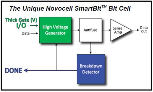
An interesting feature offered by the Novocell NVM family, based on antifuse One Time Programmable (OTP) technology, is the “breakdown detector”, allowing to precisely determining when the voltage applied to the gate (allowing programming the memory cell by breaking the oxide and consequently allowing the current to flow through this oxide) will effectively have created an irreversible oxide breakdown, the “hard breakdown”, by opposition of a “soft breakdown” which is an apparent, reversible oxide breakdown. If the oxide has been stressed during a period of time which is not long enough, the hard breakdown is not effective and the user can’t program the memory cell. Looking at the two pictures (below) help understanding the mechanisms:
- On the first, the current (vs time) is going up sharply only after the thermal breakdown is effective
- The next pictures shows the current behavior of a memory cell for different cases, and we can see that when the hard breakdown is effective the current value is about three order of magnitude higher than for a progressive (or soft) breakdown.
Thus, we can say that one of the Novocell’s differentiator is reliability. To avoid the limitations of traditional embedded NVM technology by utilizing the patented dynamic programming and monitoring process and method of the Novocell SmartBit™, ensuring that 100% of customers’ embedded bit cells are fully programmed. The result is Novocell’s unmatched 100% yield and unparalleled reliability, guaranteeing customers that their data is fully programmed initially, and will remain so for an industry leading 30 years or more. Novocell NVM IP scales to meet all NVM size and complexity challenges that grow exponentially as SoCs continue to move to advanced nodes such as 45nm and beyond.
Eric Esteve from IPNEST –
Mentor’s New Emulator
Mentor announced the latest version of their Veloce emulator at the Globalpress briefing in Santa Cruz. The announcement is in two parts. The first is that they have designed a new custom chip with twice the performance and twice the capacity. It supports up to two billion gate designs and many software engineers. Surprisingly the chip is only 65nm but Mentor reckons it outperforms competing emulators based on 45nm technology. I’m not sure why they didn’t design it at 45nm and go even faster, but this sort of chip design is a treadmill and so it is not really a surprising announcement. In fact, I can confidently predict that in 2014 Mentor will announce the 28nm version with more performance and more capacity!
Like most EDA companies, Mentor doesn’t do a lot of chip design. After all they sell software. But emulation is the one area that actually uses the tools. Since one of the big challenges in EDA is getting hold of good test data for real chips, the group is very popular in other parts of Mentor since the proprietary nature of the data is less of an issue inside the same company.
The other thing that they announced is VirtuaLAB. I assumed that this was already announced since Wally Rhines talked about it in his keynote at the Mentor Users’ Group U2U a week or two ago and I briefly covered it here. Historically, people have used an in-circuit-emulation (ICE) lab with real physical peripherals. These suffer from some big problems:
- expensive to replicate for large numbers of users
- time consuming to reconfigure (which must be done manually)
- challenging to debug
- doesn’t fit well with the security access procedures for datacenters (Jim Kenney, who gave the presentation, said he had to get special security clearance to go and get a picture inside the datacenter since even the IT guys are not allowed in)
- is never where you want it (you are in India, the peripherals are in Texas)
VirtuaLAB is a software implementation of peripherals. They run on Linux and are hardware-accurate. They can easily be shared, after all it’s just Linux. They can be reconfigured by software. You don’t need to go into the datacenter on a regular basis to reboot/reconfigure anything. Of course the purpose of all this is so that you can develop/debug and test device drivers and so on using the models. For example, here is a model of a USB 3.0 Mass Storage Peripheral (aka Thumb drive).
Afterwards I talked to Jim. He confirmed something I’ve been hearing from a number of directions. Although people have been saying for years that simulation is running out of steam and you need to switch to emulation (especially people whose job is to sell emulation hardware), it does finally seem to be true. You can’t do verification of a modern state of the art SoC including the low-level software that needs to run against the hardware, without emulation. For example, a relatively small camera chip (10M gates) requires two weeks to simulate or 20 minutes to emulate.
I asked him who his competition is. Cadence is still the most direct competition. Customers would love to be able to use an emulator at Eve’s price-point but it seems that for many designs, getting the design into the emulator is just too time-consuming. And EDA has always been a bit like heart-surgery, it’s really difficult to market yourself as the discount heart-surgeon.