I recently talked to Trent McConaghy about his book on variation-aware design of custom ICs and the #50DAC tutorial we are doing:
Winning in Monte Carlo: Managing Simulations Under Variability and Reliability.
Trent is the Solido Chief Technology Officer, an engaging speaker, one of the brightest minds in EDA, and someone who I have thoroughly enjoyed working with for the past three years.
Topic Area:Design for Manufacturability
Date:Monday, June 3, 2013
Time:11:00 AM — 1:00 PM
Location:13AB
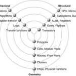
Summary: Thanks to FinFETs and other process innovations, we are still shrinking devices. But it comes at a steep price: variability and reliability have become far worse, so effective design and verification is causing an explosion in simulations. First, Daniel Nenni will do the introductions and present process variation content and analytics from SemiWiki.com. Presenter Prof. Georges Gielen, will describe CAD and circuit techniques for variability and reliability. Next, Yu (Kevin) Cao from ASU will describe how variability and aging affect bulk vs. FinFET device performance. More corners and statistical spreads will come into play, so advanced IC design tools will be needed to minimize design cycle times. Then, Trent McConaghy from Solido Design Automation, will describe industrial techniques for fast PVT, 3-sigma, and high-sigma verification. Finally, Ting Ku, Director of Engineering at Nvidia, will describe a signal integrity case study using variation-aware design techniques.
To Monte Carlo… and beyond!
Q: What is Variation-Aware Design of Custom Integrated Circuits: A Hands-on Field Guide about?
It describes a way to think about approaching design of custom ICs, such that (a) PVT and statistical variation doesn’t kill your circuit, and (b) handling the variation doesn’t chew up all your simulation resources. It doesn’t focus on the physical mechanisms causing variation, but instead examines and compares possible ways to cope with variation.
Q: What is variation-aware design?
Variation is the uncontrollable aspects of your circuit and its environment that affect the behavior of your design. These include global process variation, local process variation (mismatch), and environmental variation such as temperature and loading. While you cannot control such parameters in the real world, you *can* control them in simulations to understand their effects, and to determine designs that perform and yield well despite the variations. Variation-aware design is the act of designing circuits to meet yield, performance, and power targets despite variation.
Q: Why is variation-aware design important?
It’s not important in its own right, but it can contribute in a big way to the things that really matter. For companies, it’s the bottom line that matters, and the bottom line is affected by yield, number of chips per wafer (area), and sales (which are affected by power and performance, and time to market). For designers, what matters is making the design work, yield well, and perform well. These days, variation can profoundly yield, area, power and performance, not to mention cause respins and kill schedules. So, designing while variation-aware helps ensure that the targets for yield, area, power, and performance are hit in a timely fashion… and ultimately helps to maintain a healthy bottom line.
Q: What inspired you to write the book?
There are two main factors:
First, our customers had been asking for deep technical white papers about Solido tools, which we had taken the time to write over the years. They were very happy with those white papers, and it helped them to become super-users. But the white papers were piecemeal. We were finding that there was a simple, practical way to think about handling variation at a high level; and from that high level one could zoom into the details of handling PVT, statistical, and high-sigma variation. We thought this knowledge might be useful to our users, and also to a broader audience curious about how to address variation. We realized that a book was a great way to package this content.
Second, writing the book was a way of “giving back” to the academic community. Since I started doing CAD in the late 90s, I’ve always strived to balance industry and academia. I paused my time in industry to go back for a PhD, during which I published a fair bit, and capped off with a book. I had a good experience doing that book with Springer, so when they approached me for a new book I took it very seriously. We’re quite happy with the book’s reception from the academic community — some professors have already started using it as part of their courses. While Solido is a for-profit company, I’m glad we were able to give back to academia.
Q: What is unique about Solido’s methods?
We have three main tools, for PVT verification, 3-sigma verification, and high-sigma verification. For each of these three tools, we are the first to invent and introduce tools that are simultaneously (a) fast (b) accurate (c) scalable, and (d) verifiable [i.e. can I trust it?]. It turns out that it’s fairly easy to hit two or three of those criteria, but hitting all four is actually quite hard, and each tool took algorithmic breakthroughs. For example, in high-sigma verification there have been many publications using importance sampling algorithms, but those were typically on 6 variables. 24 variables was considered high dimension! But if you have an accurate model of process variation, with 10 local process variables per device, then even a 6T bitcell has 60 local variables! A sense amp or flip flop could hit 200. To solve the high-sigma problem in a way that achieved (a)(b)(c)(d) simultaneously, we had to completely re-think the high-sigma problem, to chop down the algorithmic computational complexity.
Q: What is the intended audience for the book?
The primary target audience is designers, who want to ship chips that work, without having to muck around too much with variation. I like to say that ‘no designer should have to know the definition of kurtosis. The book shows designers a straightforward way to think about variation to address specific variation issues, while avoiding all the ratholes along the way. For example, designers are often asked to run 100 Monte Carlo samples, but the next step is unclear. As the book describes, the way to approach MC sampling is to have a specific task or question attached, such as “does my circuit meet the 3-sigma yield target?” and appropriate tools to facilitate answering the question.
The managers and CAD managers will also find the book of value, as it can help guide them in design of their flows. For example, thanks to the deeper understanding that the book brought, some managers have been implementing PVT signoff flows where each PVT signoff run may cover >10,000 corners (at a cost of hundreds of simulations). Other managers have been implementing “true 3-sigma corner” statistical design flows. And so on.
Finally, as implied above, CAD academics will find this book of value because it provides a well-defined set of technical CAD problems, as well as baseline approaches to each CAD problem. The book can serve as a reference and starting point for their own work.
Q: How do I get a copy of the book?
All the usual suspects:
-Amazon http://www.amazon.com/Variation-Aware-Design-Custom-Integrated-Circuits/dp/146142268X
-Springer online http://www.springer.com/engineering/circuits+%26+systems/book/978-1-4614-2268-6
-The Springer booth at ISSCC, DAC, DATE, etc. Say hi to Chuck!
-It’s also been rumored that existing users of Solido software can get a copy if they ask… 🙂
Q: Will you be exhibiting at the Design Automation Conference?
Yes, readers can signup for a demo here: http://www.solidodesign.com/page/dac-2013-demo-signup/
lang: en_US