I am talking about the health of electronic and semiconductor design, which if made sound at RTL stage, can set it right for the rest of the design cycle for faster closure and also at lesser cost. Last week was the week of ITC(International Test Conference) for the Semiconductor and EDA community. I was looking forward to what ITC prescribes for the community this year and it happened such that I was able to talk to Mr. Kiran Vittal, Senior Director of Product Marketing at Atrenta. I know SpyGlass has good things about its RTL level test methodology to unveil at ITC this year, so this was an opportune time to indulge in an interesting conversation with the right expert who wrote the SpyGlass whitepaper “Analysis of Random Resistive Faults and ATPG Effectiveness at RTL”
So let’s know about what the trend is in test automation, challenges, issues, solutions,… from this conversation with Mr. Vittal –
Q: How’s the experience from ITC? What’s the top news from there?
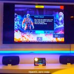
We had a very good show at ITC this year, with over 100 of the conference attendees checking out our latest advances in RTL testability solutions and product demonstrations at our exhibitor booth. We also had several dedicated meetings with existing and potential customers from leading semiconductor companies discussing how SpyGlass RTL solutions would address their key challenges.
[Customers watching SpyGlass product demonstrations]
Samsung’s Executive VP, Kwang-Hyun Kim gave the keynote address on “Challenges in Mobile Devices: Process, Design and Manufacturing”. He said that the quality of test for mobile devices is of utmost importance due to the large number (typically millions) of parts shipped. Any degradation in quality can badly impact the rejection ratio which can affect the bottom line as well as the reputation of the particular company.
One of the best paper awards was also related to RTL validation –
ITC 2012 Best Student Paper Award: Design Validation of RTL Circuits Using Evolutionary Swarm Intelligence by M. Li, K. Gent and M. Hsiao, Virginia Tech
Q: What is the industry trend? Is it converging towards RTL level test?
The industry trend for deep submicron designs is to ship parts with the highest test quality, because new manufacturing defects surface with smaller geometry nodes. These defects need additional tests and the biggest concerns are the quality and cost of testing to meet the time-to-market requirements. Every semiconductor vendor performs at-speed tests at 45nm and below. The stuck-at test coverage goal has also increased from ~97% to over 99% in the last couple of years. The other concern has to do with design size and the large quantity of parts being shipped in the mobile and handheld space and the danger of having rejects for missing manufacturing defects due to the lack of high quality tests.
The only way to get very high test quality is to address testability at an early stage in the design cycle, preferably at RTL. The cost of test can be reduced by reducing the test data volume and test time. This problem can also be addressed by adhering to good design for test practices at the RTL stage.
Q: So, there must be great interest in SpyGlass test products which work at RTL level?
Yes, there is great interest in Atrenta’s solution for addressing testability at the RTL stage. We have a majority of the large semiconductor companies adopting our RTL testability solution. They say that by adopting SpyGlass testability at RTL, they are able to significantly shorten design development time and improve test coverage and quality.
Q: What’s the benefit of using SpyGlass? How does it save testing time? What kind of fault coverage does it provide compared to ATPG?
Fault coverage estimation at RTL is very close to that of ATPG, typically within 1%.
SpyGlass DFT has a unique ability to predict ATPG (Automatic Test Pattern Generation) test coverage and pinpoint testability issues as the RTL description is developed, when the design impact is greatest and the cost of modifications is lowest. That eliminates the need for test engineers to design test clocks and set/reset logic for scan insertion at the gate level, which is expensive and time consuming. This significantly shortens development time, reduces cost and improves overall quality.
The test clocks in traditional stuck-at testing are designed to run on test equipment at frequencies lower than the system speed. At-speed testing requires test clocks to be generated at the system speed, and therefore is often shared with functional clocks from a Phase Locked Loop (PLL) clock source. This additional test clocking circuitry affects functional clock skew, and thus the timing closure of the design. At-speed tests often result in lower than required fault coverage even with full-scan and high (>99%) stuck-at coverage. Identifying reasons for low at-speed coverage at the ATPG stage is too late to make changes to the design. The SpyGlass DFT DSM product addresses these challenges with advanced timing closure analysis and RTL testability improvements.
SpyGlass MBIST has the unique ability to insert memory built-in self test (BIST) logic at RTL with any ASIC vendor’s qualified library and validate the new connections.
Q: What’s new in these products which caught attention at ITC?
We introduced a new capability at ITC for analyzing the ATPG effectiveness early at the RTL stage, especially for random-resistive or hard-to-test faults.
ATPG tools have been traditionally efficient in generating patterns for stuck-at faults. The impact on fault coverage, tool runtime and pattern count for stuck-at faults is typically within reasonable limits.
However, the impact of “hard-to-test” faults in transition or at-speed testing is quite large in terms of pattern count, runtime or test coverage. This problem can now be analyzed with the SpyGlass DFT DSM product to allow RTL designers to make early tradeoffs and changes to the design to improve ATPG effectiveness, which in turn improves test quality and overall economics. Details can be seen in our whitepaper on Random Resistive Faults.
Q: Any customer experience to share with these products?
Our customers have saved at least 3 weeks of every netlist handoff by using SpyGlass DFT at the RTL stage. The runtime of SpyGlass at RTL is at least 10 times faster than running ATPG at the netlist level. Our customers have claimed about a 25x overall productivity improvement in using SpyGlass at RTL vs. other traditional methods.
This interaction with Mr. Vittal was much focused on testing aspects of Semiconductor Design. After this conversation, I did take a look at the new whitepaper on Random Resistive Faults and ATPG Effectiveness at RTL. It’s worth reading and knowing about effective methods to improve fault coverage.