You are currently viewing SemiWiki as a guest which gives you limited access to the site. To view blog comments and experience other SemiWiki features you must be a registered member. Registration is fast, simple, and absolutely free so please, join our community today!
FPGA-based prototyping offers advantages such as high-speed operation, real-world environment testing, and parallel execution that cannot be matched by software simulations alone. It enables developers to validate their designs and initiate software development long before the final silicon is ready. At the same time, prototyping is not merely just an FPGA board, and many factors need to be considered when it comes to rapid and effective implementation. Accelerating FPGA prototyping requires a combination of advanced hardware capabilities, improved design methodologies, efficient debugging tools, and reliable software automation. By leveraging these approaches, engineers can significantly reduce prototyping time while maintaining accuracy and performance.
The Challenges of Prototyping for SoC Development
One of the major hurdles in SoC prototyping is ensuring a realistic testing environment that accurately simulates real-world chip behavior. Additionally, challenges such as managing partitioning for large-scale designs and achieving stable communication between high-speed and low-speed devices add to the complexity. Without the right tools and strategies, development teams face significant delays and increased risk during the prototyping phase, which can impact their ability to meet project deadlines and deliver quality products to the market.
Innovative Approaches to Overcoming Prototyping Hurdles
To address these challenges, several innovative approaches have emerged. Flexible interfaces, such as configurable daughter boards, enable rapid connection to external devices and mimic real-world conditions, allowing developers to validate designs in realistic environments. Speed adapter solutions ensure seamless communication between devices operating at different speeds, which is critical for high-speed interfaces like PCIe or advanced memory standards like LPDDR4/5. Co-simulation tools and reference designs streamline the debugging process by facilitating efficient data exchange and providing pre-validated solutions, reducing the need for custom development. Furthermore, optimized design partitioning and FPGA interconnecting topology play a vital role in managing the complexities of large-scale SoC designs, allowing for iterative mapping of components while maximizing system scalability.
S2C’s Prodigy Prototyping Solutions
S2C’s Prodigy Prototyping Solutions address key challenges in FPGA-based SoC prototyping through flexible hardware, reliable software tools, and streamlined processes.
Flexible Daughter Boards for Seamless Integration
S2C’s Prodigy platform features a vast library of daughter boards supporting applications ranging from communications and SoC to storage and multimedia, including various gigabit Ethernet interfaces, QSFP28/QSFPDD, PCIe, USB, LPDDR4/DDR4, QSPI, EMMC, MIPI D-PHY and HDMI. These modular daughter boards, pre-validated to meet industry standards, simplify system setup and reduce development risks.
Speed Adapter and Memory Models to Bridge the Gap
To overcome the limitations of FPGA-based systems in handling high-speed protocols or the latest memory interfaces, S2C offers speed adapter and memory model solutions to support the device under test in the FPGA environment. This is particularly useful in validating PCIe subsystem not running at real-world speed or advanced memory controllers such as DDR5/HBM, where FPGA vendors often lack suitable PHY IPs. S2C’s PCIe speed adapter can act as a gear shift between two different PCIe speeds while memory models allow customers to validate LPDDR5/DDR5/HBM based memory controllers by bridging gaps to FPGA’s DDR4 PHYs, addressing critical bottlenecks.
High Productivity Toolchain to Streamline Large-scale SoC Designs
Software/hardware co-development with ProtoBridge™: ProtoBridge enables high-throughput data exchange between FPGA prototypes and PC hosts at speed up to 4GB/s utilizing PCIe connectivity. With ready-to-use C APIs on host PC and bridging AXI-4 master/slave IPs running in the DUT, large data such as videos, software applications or operating systems can be uploaded with ease. ProtoBridge is also a critical building block for co-simulation and other co-development applications.
Remote Runtime Management with PlayerPro – Runtime (PPro-RT): Prototyping can be remotely managed and download designs over Ethernet/USB by PPro-RT. With hardware self-tests, virtual I/O tools, and design resource access, it simplifies multi-system management, ensuring effective hardware validation and streamlined firmware testing.
Deep trace and multi-FPGA debugging with PlayerPro – DebugTime (PPro-DT): PPro-DT allows users to pre-select the signals to be observed before compilation and define the trigger conditions to start a data capture. During runtime, the selected signals are captured and stored in an external DDR4 memory for analysis.
Multi-FPGA prototyping with Player Pro – Compile Time (PPro-CT): PPro-CT is a timing-driven partitioning software enables one-click flow from RTL to bitstream, simplifying the steps of large design partitioning with features such as system level STA, high-performance TDM assignment and incremental compilation.
The Benefits of S2C’s Solutions
By providing a near-realistic environment for software validation, S2C’s customers reduce the likelihood of costly rework after silicon fabrication, ensuring a smoother transition to final production. Development teams improve efficiency by leveraging pre-validated components and automated tools, which minimize errors and streamline the prototyping process. The tools also save engineering resources, allowing developers to focus on innovation rather than labor-intensive setup and troubleshooting tasks. Faster time-to-market is achieved as these solutions significantly reduce the time required for debugging and verification, enabling teams to meet tight deadlines.
Summary
The success of FPGA-based prototyping hinges on overcoming several key challenges. By integrating flexible interfaces, speed adapter solutions, advanced co-simulation tools, and high productivity toolchain, S2C’s Prodigy Prototyping Solutions address these challenges head-on. The S2C Prodigy platform empowers development teams to reduce risk, validate designs more efficiently, and deliver products to market faster, making it an invaluable tool in the fast-paced world of chip design.
The moral of today’s story is that to succeed in a late-adopter market, sometimes you just have to wait for the market to catch up (assuming you have a strong early adopter market to buy your product today). I have been working with Arteris for 6+ years now promoting their NoC technology, and there was never any question that they offer significant value for design teams building big, complex systems-on-chip connecting multiple IPs through extensive networks. Such systems include application processors and, more recently, AI systems for automotive applications. Lower-end designs, commonly MCUs, had been more resistant to the benefits of Arteris technology. But as AI, safety, and security are becoming just as important in MCUs as elsewhere, even MCU design teams are rethinking their earlier strategies.
Evolving MCU demands
Historically, MCUs have served relatively bounded objectives like control units in car engines and home appliances. The architecture was comparably simple: an 8-bit processor, memory, peripherals, timers, counters. One initiator, a few targets, easily satisfied by crossbar switch interconnect. Design support teams often built their own generators for this kind of interconnect. A small number even built their own NoC generators to handle more complex system interconnects.
Now even legacy in-house generators are coming under pressure, in part through competitive and regulatory requirements and in part to meet scalability expectations. AI is everywhere, as much in MCUs as anywhere else to support intelligent sensing. Automation demands for smart homes, cars, cities, factories, all require smart MCUs with communication support. Many must also prioritize safety and security, all at very constrained cost and power demand per unit. Cities and factories planning to deploy thousands of devices want unit prices around a few dollars at most and even lower maintenance costs.
MCUs are growing up to meet these needs; now it’s not always easy to tell where MCUs end and SoCs begin. According to Andy Nightingale (VP Product Management and Marketing, Arteris), MCUs span a long tail beyond SoCs, from complex all the way down to simple devices. Simple MCUs still have their uses where cost is more important than adding features (simple toys or basic home thermostats, for example), but above wherever that breakpoint might be, more functions must be supported on-chip and that invariably requires NoC connectivity.
The drivers to mainstream NoCs
What is motivating change at the simpler end of this MCU range? In part, power reduction. Networks burn power even when there’s no traffic, a fact easy to overlook when concentrating on minimizing power in endpoint IPs. This power component alone can be an important overhead, unless you are using a network like Arteris FlexNoC which supports power domain switching and DVFS within the network.
Safety standards have become another driver. If the MCU is going into any safety-critical application (car, aircraft, industrial robotics, …) you must demonstrate compliance to applicable standards, again as much for the network as for the endpoint IP. Arteris has already done the groundwork against both ASIL B and ASIL D for automotive applications.
At higher complexities, many requirements making NoCs essential in SoC design have become just as relevant in MCU design. Support for multiple protocols (AXI, ACE-lite, ACE, CHI, APB, etc.) is unavoidable in designs using both legacy and 3rd party IP, and acceptable performance for systems with multiple initiators and targets is only possible through the packetization offered by NoCs.
AI accelerators, multicore processors, and again performance are pushing new network topologies: mesh, tree, Clos, even crossbars in some cases, demanding NoC generators with track records to provide support across this range. Meanwhile, network standards continue to evolve. In debug and parametric modeling, support for ATB 128-bit trace and now DVM 8.1 have become essential. AMBA 5 now supports “stashing” to improve memory utilization, latencies, and bandwidths, here also requiring support from the NoC generator. High-end goals can only be guaranteed with networks that constantly track these new demands.
For implementation, it is now clear that complex NoC design must be physically as well as architecturally aware right from the outset. Bus widths and serialization options can be optimized early on against rough floorplan concepts and later fine-tuned against realistic floorplans to best optimize area/performance tradeoffs. Just as logical/physical co-design appeared years ago in physical synthesis for block design, now the same need has become unavoidable in full system design.
Strategic planning for scalability
No design is an island, as some reuse expert might have said. What we build today must also factor into tomorrow’s plan for larger or repurposed designs. Or reuse may go in the opposite direction. Auto OEMs may first design a system for the high end of a car range, with intent to deploy the same system or a derated version in lower-end models in the future. In support of these goals, it is necessary to plan for a design infrastructure that can span seamlessly from low-end MCUs to high-end MCUs to SoCs, without need for fundamental network redesign.
Between the intrinsic flexibility of NoC-based networks and physically aware design, Arteris networks can easily span this range (since they are already widely deployed in high-end SoC design flows). Hierarchical NoCs are already as commonplace as hierarchical crossbar switches, so reuse methods are also well-proven. It seems pretty clear that NoC architectures are the way to go for scalability.
You can learn more about this topic HERE, the Arteris non-coherent FlexNoC architecture HERE, and their coherent Ncore architecture HERE.
CES 2025 was held last week in Las Vegas. We at Semiconductor Intelligence attended for our tenth CES. The event had over 140,000 attendees and over 4,500 exhibitors.
U.S. Consumer Electronics Market
Brian Comiskey of the Consumer Technology Association (CTA) presented on technology trends in 2025. The key theme was advances in AI and connectivity will lead to major changes in enterprise operations, consumer electronics, energy, mobility, smart homes and media. Comiskey presented CTA’s forecast for the U.S. consumer electronics market.
After strong growth in 2021 due to recovery from the pandemic, the overall U.S. electronics market fell in 2022 and 2023. The market turned positive in 2024, with 2.5% growth. The expectation is for stronger growth in 2025 at 3.2%.
However, there is much uncertainty about the outlook in 2025. U.S. President-elect Donald Trump has proposed new tariffs on imports to the U.S. Two proposals are:
• A 60% tariff on imports from China and a 10% tariff on other imports.
• A 100% tariff on imports from China and a 20% tariff on other imports.
The CTA conducted a study on the potential impact on the U.S. electronics market if these tariffs are enacted. Using the lower-tariff scenario, the price increases to consumer and the change in consumption due to the higher prices are:
Under the higher-tariff scenario, CTA estimates consumption of laptops & tablets would drop 68% and consumption of smartphones would drop 54%. Thus, the CTA forecast of 2.6% growth in the U.S. electronics hardware market in 2025 could instead be a major double-digit decline.
CES 2025 Themes
AI was the overriding theme of CES 2025. The kickoff keynote was by Jansen Huang, CEO of Nvidia, the dominant AI chip provider. Huang said AI will enable major advancements in technology. Every engineer, programmer and content creator will need an AI assistant to do their job effectively. AI has allowed advances in real-time image rendering which will have a major impact on video games, movies and television. AI will analyze physical world data to train robots. Huang predicted robots will become the largest technology industry in the not-too-distant future.
Nvidia’s Jensen Huang with AI enabled robots
Delta Airlines’ keynote was held in the Las Vegas Sphere, a 18,600-seat venue with the world’s largest video screen at 160,000 square feet. Delta Airlines CEO Ed Bastian spoke about using AI to analyze customer feedback and make air travel more personalized. Delta will partner with Joby to provide electric vertical take-off and landing (VTOL) aircraft to transport passengers from city centers to airports. Delta is also partnering with Uber to connect transportation to the airport with airline reservations.
Delta’s Ed Bastian in the Las Vegas Sphere
Samsung’s press conference emphasized home AI through its SmartThings system. Samsung has over 340 partners working on Smart Things applications. The goal is to use SmartThings to integrate and control TVs, appliances, smartphones, connected devices, lighting, heating and air conditioning. Samsung is working with Hyundai on automotive AI for electric vehicles. In a departure from the past, Samsung did not use the press conference to introduce any new TVs, smartphones, or appliances.
Among the other major consumer electronics companies, LG Electronics’ booth had a similar theme to Samsung – the AI home. Sony’s booth focused on a few areas including gaming, cameras and video entertainment.
Vehicle Technology
The West Hall of the Las Vegas convention center (LVCC) was devoted to Vehicle Technology and Advance Mobility. TIER IV exhibited an autonomous bus which is currently in operation in Japan. May Mobility showed an autonomous vehicle (AV) built using a Toyota vehicle. May will introduce AVs in partnership with Lyft in Atlanta later in 2025. Oshkosh displayed electric trucks including a fire truck, garbage truck and a delivery vehicle for the U.S. Postal Service. John Deere featured autonomous equipment for farming and construction. Chinese company Zeekr drew a crowd with its EVs featuring its Golden Battery which charges from 10% to 80% in 10.5 minutes. Waymo exhibited its AVs in partnership with Zeekr and Hyundai.
Oskosh electric fire truck
Interestingly, most of the major automakers did not have exhibits. Honda displayed its EV concept models, the Honda 0 Saloon and SUV. BMW showcased its Panoramic iDrive display which will be in all BMW models by the end of 2025. None of the other major automakers had displays at CES.
Robots
Robots were prominent at CES 2025. Robots on display performed tasks such as making coffee, serving food, greeting and providing information. Open Droids is introducing a series of robots to perform more complex household tasks such as unloading dishwashers, doing laundry, and cleaning. Numerous types of electric personal transportation were on display, including electric bikes, scooters, and even an electric surfboard.
CES 2025 continued the shift from consumer electronics being driven by traditional products such as TVs, smartphones and appliance to AI-enabled new products such as robots, electric vehicles and autonomous transportation. As a result, we are seeing much of the innovation being driven by start-up companies rather than large consumer electronics companies.
Semiconductor Intelligence is a consulting firm providing market analysis, market insights and company analysis for anyone involved in the semiconductor industry – manufacturers, designers, foundries, suppliers, users or investors. Please contact me if you would like further information.
Bill Jewell
Semiconductor Intelligence, LLC
billjewell@sc-iq.com
Chiplets continue gaining momentum, fueled in large part by applications for AI and 5G/6G RFICs. Keysight has a strong presence at this year’s Chiplet Summit in Santa Clara, which includes Simon Rance in a super panel discussing “Chiplets: The Key to Solving the AI Energy Gap” and Nilesh Kamdar with a keynote on “Using Design-to-Test Workflows and Managing the IP Lifecycle in Chiplet Designs”, as well as several technical talks. Keysight previewed some of its material for the conference, focusing on three aspects of its chiplet integration solutions: system-level electrical layer analysis, a compliance testing strategy to characterize golden die and die-to-die channels, and engineering lifecycle management for chiplet design.
System-level analysis of signal integrity crucial for chiplets
Chiplet designers are facing many challenges in creating die-to-die interconnects. Do teams align with a specification, such as Universal Chiplet Interconnect Express (UCIe), Bunch of Wires (BoW), or others? Do they follow the details of a chosen specification closely, seeking to capture the economic benefits of interoperability, or do they customize some features, tuning interconnects to optimize performance and power consumption? In any chiplet design scenario, system-level chiplet signal integrity analysis determines a design’s outcome. Packaging for 3D heterogeneous interconnect (3DHI), using standard or advanced packages specified in UCIe, becomes more than a mechanical convenience, affecting high-bandwidth signals.
Preventing suboptimization of one signal metric while potentially degrading others calls for detailed, system-level electrical layer analysis, evaluating all metrics simultaneously. Keysight’s Chiplet PHY Designer, an extension to Keysight Advanced Design System (ADS), provides robust system-level signal integrity analysis for chiplet interconnects, including UCIe and BoW. It updates its analysis incrementally as schematic and layout details change.
Tim Wang Lee, Ph.D., Signal Integrity Application Scientist at Keysight, presents the topic “Fast Track Chiplet Integration with Streamlined UCIe Electrical Layer Analysis” in the Integration sessions. “UCIe specifies the voltage transfer function (VTF), forward clocking, eye mask equalization, loss, and crosstalk level,” he says. “Our software does the work by setting up TX and RX termination equalization and analyzing and visualizing VTF crosstalk and loss masks for different data rates.”
Dr. Tim also says the visualization tools in Chiplet PHY Designer help spot the root cause of issues, such as insufficient trace spacing creating coupling and excessive crosstalk or channel lengths contributing to losses. He emphasizes that while Chiplet PHY Designer is UCIe-aware, it also handles analysis for BoW or customized die-to-die interconnect links.
Die-to-die interconnect test and characterization
UCIe leans heavily upon work done for its board-level predecessor, PCIe, with modifications recognizing its die-to-die context. However, there is one significant difference – compliance testing. PCIe is famous for its plugfests, where teams can take chips designed with mature PCIe IP blocks, mount them on circuit boards, install them in systems, and stage physical and protocol measurements using signal generators, oscilloscopes, and bit error rate testers. UCIe presents a different challenge since fabricating a chiplet prototype is much more expensive than making a board prototype, and limited test point visibility can make probing infeasible.
Pedro Merlo, Manager of Strategic Planning at Keysight, comes from the test instrumentation side of the house and has been focusing on die-to-die interconnects for the past two years. “Keysight is a proud contributor to UCIe and BoW, the two most prominent chiplet interconnect standards,” says Merlo. “The vision is to base compliance testing at the physical and protocol layers on a ‘golden’ die.” But does such a die exist, especially for customized link designs? For an open chiplet ecosystem to develop, at least three components – one die, one interconnect structure, and another die that completes the link – must be testable standalone and swappable for another test article.
Merlo’s tutorial in the Pre-Con D: Introduction to Die-to-Die Interfaces session shares some in-progress thinking where Keysight’s unified measurement science – equivalent methods between test hardware and EDA software – comes into play. “We can use our high-precision benchtop test equipment to characterize a chiplet’s built-in self-test (BIST) and measure transmitter amplitude, slew rate, jitter, skew, equalization, sensitivity, and more,” he begins. “Our objective is to test as much as possible to reduce the uncertainty, especially after packaging, when test points are no longer accessible.”
“We’re proposing extracting channel characteristics and factoring them into measurements made at the far end of the transmitter, then using those characteristics in a model for end-to-end tests,” Merlo continues. “The approach adds test points to a substrate, makes measurements there, then subtracts out channel effects to see what the signal looks like at the receiver microbump.”
Merlo points out that BIST results can tell designers that a link works but not how much margin it has or where a problem might be. Decomposing the BIST into two phases provides a method for examining links closely.
More importantly, decomposing the BIST paves the way for simulations with robust models to produce results equivalent to measurements. “By breaking the link into pieces and ensuring each one works and meets specifications, we get better information,” Merlo concludes.
Engineering lifecycle management for chiplet design
Considering both electrical and mechanical nuances, chiplet design presents a more significant enterprise opportunity for engineering lifecycle management (ELM) than SoC design. While today’s focus on chiplet design is internal, teams may soon be considering if third-party chiplets are candidates for integration. There’s also reuse of chiplets to consider, and if an organization has more than one design team, there needs to be an easy way to store and share design information across teams.
“Think of chiplets as systems,” says Pedro Pires, ELM Solutions Engineer at Keysight. “Chiplet design carries system engineering connotations – there are die, interposers, packages, and artifacts around each component, some internally sourced and some procured from third parties.” Pires says a common chiplet design scenario will see teams starting with specifications, diving into a catalog with parameterized search and compare of components, and creating a bill of material (BOM) with built-in traceability of assets.
Metadata around chiplets in Keysight Design Data Management (formerly known as Cliosoft SOS) can include what versions exist, where they are in use, and their technical characteristics, including electrical, mechanical, and application programming interface (API) information, making it easy to highlight differences. “HUB can provide critical alerts such as release conflicts, where one bill of material contains different versions of a chiplet somewhere in its hierarchy, or notify designers of a newer version,” adds Pires.
There may be more steps for designers than just grabbing an asset from the catalog. Pires points out that selecting third-party chiplets may require team members to execute non-disclosure and licensing agreements. Keysight ELM implements workflows as a mechanism to automate approval and enforcement policies, with built-in activity reporting for internal and third-party audits. Beyond these customizable workflows, granular access controls can gate access to resources based on user characteristics, roles, or locations, which is essential for expert control scenarios.
Keysight ELM introduces a data-agnostic methodology for managing the entire lifecycle of chiplets and offers creative ways for various roles beyond design teams to share and manage information. It integrates seamlessly with many chiplet design tools, including Keysight ADS and Cadence Virtuoso, via a REST API. It also connects with familiar tools like Jama, JIRA, Bugzilla, Confluence, and more.
Learn more at Chiplet Summit 2025
The complete technical presentations will reveal more details for Chiplet Summit 2025 conference attendees. In addition to the speaking slots on the program, exhibitor attendees can see Keysight’s chiplet integration solutions in booth #307, including the presentation on ELM. For more information on Chiplet PHY Designer, Keysight Design Data and IP Management, and the Chiplet Summit program and registration, please visit the following:
Part 1 of 2 – Essential Performance Metrics to Validate SoC Performance Analysis
Part 1 provides an overview of the key performance metrics across three foundational blocks of System-on-Chip (SoC) designs that are vital for success in the rapidly evolving semiconductor industry and presents a holistic approach to optimize SoC performance, highlighting the need for balancing these metrics to meet the demands of cutting-edge applications.
Prolog – SoC Performance Validation: Neglect It, Pay the Price!
In today’s technology-driven world, where electronics and software are deeply intertwined, the ability to estimate performance (as well as power consumption) ahead of tape-out has become a crucial factor in determining a product’s success or failure. Below are some real-world examples of failures that could have been avoided by pre-silicon performance validation:
A hardware bug in the coherent interconnect fabric of an Android smartphone chip slipped through into the delivered product causing all caches to flush and forcing the Android system to reboot. This oversight led to a recall with significant financial losses for the developer.
A hidden firmware bug triggered sudden and random drops in datacenter utilization in a range of 10% to 15%, resulting in sizable financial losses.
An expert analysis of the October 22, 2023, GM Cruise autonomous vehicle accident in San Francisco revealed that the AD controller failed to detect a pedestrian lying on the asphalt after a hit-and-run accident. The failure occurred because latency exceeded the specified limits for detecting and responding to moving targets. As a result, GM suspended driverless operations of its Cruise vehicles for several months and incurred significant penalties.
After multiple years of unsuccessful attempts to design a high-performance GPU for a mobile chip, a major semiconductor company was forced to adopt a competitor’s solution, incurring substantial costs.
These costly malfunctions and/or missed target specifications could have been avoided through comprehensive pre-silicon performance analysis.
SoC Performance Metrics Critical for Success
Achieving performance targets in today’s cutting-edge SoC designs is critical to determining the success or failure of a product. When looking at design trends, in particular for AI, designs are running into the memory and interconnect walls as shown in the following figures.
Fig 1: Memory Wall (Source: AI and Memory WallFig 2. Interconnect Wall (Source: AI and Memory Wall
For instance, when evaluating SSD storage, developers focus on two metrics: the read/write speed of the SSD and its total capacity. These figures are crucial for memory companies, especially as the volume of data being transferred continues to grow exponentially. The ability to quickly move data off the chip is vital. In the data center market, memory accounts for roughly 50% of resource usage, acquisition cost, and power consumption, that is half of their investment into purchasing memory, maintaining it with sufficient power, and ensuring enough capacity to support parallel memory accesses. As a result, memory performance often becomes a bottleneck.
As another example, AI market performance hinges on the rapid processing of algorithms, which is largely determined by the speed to retrieve input data from memory and to offload results to memory. This is crucial for inference tasks, where real-time decisions depend on quickly retrieving input data and storing results. In automotive applications, for instance, swift data access is essential for split-second decisions like pedestrian detection. Conversely, the faster the data offloading occurs, the more efficient the data handling become, especially in training environments where large datasets must be constantly moved between cores and memory.
Regardless of the application, ultimately three key metrics define performance in SoC designs:
Latency
In SoC designs, latency refers to the time elapsed between the request of a data transfer or of an operation and the delivery of the data or the completion of the operation.
In any SoC design the architectures of three fundamental functional blocks determine the latency of the entire design:
Memory Latency: The delay in accessing data in memory. Memory latency is influenced by memory type, memory hierarchy structure, and clock cycles required for access, typically interdependent.
Interconnect Latency: The time it takes for data to travel across the SoC’s fabric interconnecting one component to another. Critical attributes in an interconnect architecture include number of hops, congestion dependency, protocol overhead.
Interface Protocols Latency: The delay in communicating with external devices through peripheral interfaces. Latency in interface protocols ranges widely from several nanoseconds (PCIe) to microseconds (Ethernet).
High latency in data transfer or response time degrades system performance, especially in real-time or high-performance applications such as AI processing, automotive systems, real-time communications, and high-speed computing.
Bandwidth
In SoC designs, bandwidth refers to the maximum data transfer rate between different components within a chip or between a chip and external devices.
Like latency, the architectures of same three fundamental functional blocks determine the bandwidth of the entire design:
Memory Bandwidth: The data transfer rate between processing units and memories. Measured in GigaBytes per second (GB/s) is influenced by factors such as memory type, bus width, and clock speed.
Interconnect Bandwidth: The data transfer rate between various blocks and subsystems through interconnect fabric like buses or crossbars.
Interface Protocols Bandwidth: The data transfer rate in the communication channels with external devices through peripheral interfaces.
Low bandwidth in an SoC design leads to data congestion. Conversely, high bandwidth improves performance, particularly for data-intensive tasks such as AI/ML processing. Achieving high bandwidth involves optimizing the architecture of memory subsystems, interconnects, and communication protocols within the SoC.
Latency optimization is often balanced with bandwidth optimizations to achieve optimal overall performance.
Accuracy
In SoC designs, data transfer accuracy refers to correctness and reliability of data as it moves between different components within the SoC or between the SoC and external devices.
Data transfer errors can be caused by several factors: congestion, overflow, underflow, incorrect handshakes, noise, interference, crosstalk, signal degradation, or electromagnetic interference (EMI) impacting signal integrity.
Inaccuracies in data transfer can lead to system failures, crashes, loss of data, incorrect computations, especially critical in systems requiring high reliability, such as automotive, medical, or AI-based systems. Ensuring data transfer accuracy is a fundamental aspect of SoC design.
Holistic Approach to SoC Performance Optimization
In today’s highly competitive and demanding SoC design landscape, optimizing the three core attributes that define performance—latency, bandwidth, and accuracy—has become an absolute necessity. This optimization extends beyond hardware alone, and it includes firmware as well. This is especially true for leading-edge SoC designs, from AI-driven systems to high-performance computing and real-time applications as self-driving vehicles.
Achieving optimal performance in SoCs requires a holistic approach that balances hardware and software considerations.
Addressing Performance in Memory Architectures
Memory architecture is central to SoC performance, directly affecting both latency and bandwidth. Memory access speeds and capacity are critical for ensuring that processing cores are not starved of data, particularly in high-throughput applications.
Advanced memory architectures are designed to strike a balance between low-latency access and high-bandwidth memory operations, delivering both speed and capacity required for today’s demanding workloads. For example, LPDDR5 (Low Power Double Data Rate 5) and HBM3 (High Bandwidth Memory 3) represent cutting-edge DRAM technologies that have been engineered to maximize performance in power-constrained environments, such as mobile devices, as well as high-performance computing applications.
LPDDR5 offers improvements in power efficiency and data throughput, enabling mobile SoCs and embedded systems to access memory faster while consuming less power. Meanwhile, HBM3 delivers unparalleled bandwidth with stacked memory dies and a wide bus interface, making it ideal for high-performance applications like AI accelerators, GPUs, and data center workloads. By integrating memory closer to the processor and using wide memory buses, HBM reduces the distance that data must travel, minimizing latency while enabling vast amounts of data to be accessed concurrently, and ensures that multiple processing cores or accelerators can access data simultaneously without bottlenecks.
Shared memory architectures enable different processing units—such as CPUs, GPUs, and specialized accelerators—to access the same pool of data without duplicating it across separate memory spaces. This is especially important for heterogeneous computing environments where different types of processors collaborate on a task.
Cache coherency protocols in multi-core systems guarantee that data remains consistent across different cores accessing shared memory. Protocols like NVMe (Non-Volatile Memory Express), UFS (unified file storage), MESI (Modified, Exclusive, Shared, Invalid) and MOESI (Modified, Owned, Exclusive, Shared, Invalid) are commonly used to maintain cache coherency, ensuring that when one core updates a piece of data, other cores working on the same data are immediately notified and updated.
Addressing Performance in Interface Protocols Architectures
Interface protocols manage the data traffic between the SoC and its external world, playing a vital role in maintaining SoC performance by directly influencing both latency and bandwidth.
High-performance interface protocols like PCIe and Ethernet are designed to maximize data transfer rates between the SoC and external devices preventing data congestion and safeguarding that high-performance applications can consistently meet performance requirements without being throttled by communication delays.
Emerging standards like CXL (Compute Express Link) and Infinity Fabric are designed to enhance the interconnectivity between heterogeneous computing elements. CXL, for instance, enables high-speed communication between CPUs, GPUs, accelerators, and memory, improving not only data bandwidth but also interconnection efficiency. Infinity Fabric, used extensively in AMD architectures, provides a cohesive framework for connecting CPUs and GPUs, ensuring high-performance data sharing and coordination across computing resources.
In the AI acceleration space, Nvidia currently dominates in part due to its superior interface protocols, such as InfiniBand and NVLink. InfiniBand, known for its low-latency, high-bandwidth performance, is widely used in data centers and high-performance computing (HPC) environments. Nvidia’s NVLink, a proprietary protocol, takes data transfer to the next level by achieving rates of up to 448 gigabits per second. This allows for fast data movement between processors, memory, and accelerators, which is essential for training complex AI models and running real-time inference tasks.
Addressing Performance in Interconnect Networks
Interconnect networks play a pivotal role in SoC designs, acting as the highways that transport data between different components. As SoCs become more complex, with multiple cores, accelerators, and I/O components, the interconnect architecture must be capable of supporting massive parallelism and enabling efficient workload distribution across multiple processors and even distributed systems.
To achieve optimal performance, the interconnect must be designed with throughput maximization and low-latency communication in mind. As data movement becomes increasingly complex, the interconnect network must handle not only the sheer volume of data but also minimize bottlenecks and contention points that can slow down performance.
Interconnect architectures developed for performance such as On-Chip Networks (NoC) and Advanced Microcontroller Bus Architecture (AMBA) reduce contention and minimize communication delays between cores, memory, and peripheral components, and ensure that data is routed efficiently between components.
High-performance interconnect architectures like Network-on-chip (NoC) and Advanced Microcontroller Bus Architecture (AMBA) have been developed to meet these demands. Networks on Chip (NoC) are designed to scale with the growing complexity of SoCs, offering high levels of parallelism and flexible routing to reduce contention and enable a modular design approach, where multiple components can communicate simultaneously without overloading shared buses or memory channels, thereby preventing data congestion and minimizing latency.
Similarly, AMBA (Advanced Microcontroller Bus Architecture) has become a standard for connecting processors, memory, and peripherals within an SoC. By incorporating advanced features such as burst transfers, multiple data channels, and arbitration mechanisms, AMBA helps reduce communication delays and ensures that data is routed efficiently across the SoC.
In addition to NoC and AMBA, newer interconnect solutions are emerging to address the growing demand for more advanced performance optimization. Coherent interconnects, such as Arm’s Coherent Mesh Network (CMN), allow multiple processors to share data seamlessly and maintain cache coherence across cores, reducing the need for redundant data transfers and improving overall system efficiency.
Addressing Performance in Firmware
Performance tuning goes beyond optimizing the three essential hardware blocks, and it must also encompass the lower layers of the software stack, including bare-metal software and firmware. These software layers are integral to the system’s overall performance, as they interact with the hardware in a tightly coupled, symbiotic relationship. Bare-metal software and firmware act as the interfaces between the hardware and higher-level software applications, enabling efficient resource management, power control, and hardware-specific optimizations. Fine-tuning these layers is crucial because any inefficiencies or bottlenecks at this level can significantly hinder the performance of the entire system, regardless of how well-optimized the hardware may be.
One of the key benefits of firmware optimization is its ability to unlock performance gains without requiring changes to the physical hardware. For instance, firmware updates can be deployed to improve resource allocation, reduce latency, or enhance power efficiency, leading to significant performance improvements with minimal disruption to the system. This is especially critical in embedded systems, IoT devices, and SSDs, where firmware governs how efficiently data is processed and managed.
Beyond storage devices, firmware optimization is beneficial in domains as networking equipment, GPUs, and embedded systems.
Conclusions
SoC designs are the backbone of numerous technologies, from smartphones and autonomous vehicles to data centers and IoT devices, each requiring precision-tuned performance to function optimally. Falling short of performance goals can lead to higher costs, delayed time-to-market, and compromised product quality, ultimately affecting a company’s competitiveness in the market. Conversely, hitting these targets means faster, more reliable products that stand out in a crowded tech landscape.
As design cycles shorten and market pressures intensify, achieving performance metrics is no longer optional—it’s a necessity for any successful SoC project.
Read Part 2 of this series – Performance Validation Across Hardware Blocks and Firmware in SoC Designs
Advantest Corporation, a world-leading supplier of semiconductor test equipment, has been honored with the Excellent Performance Awardat the 2025 Taiwan Semiconductor Manufacturing Company (TSMC) Supply Chain Management Forum. This recognition, presented by one of the semiconductor industry’s most influential companies, marks a major milestone in Advantest’s ongoing efforts to strengthen collaboration with TSMC and extend its impact across the global semiconductor supply chain.
The award was bestowed during TSMC’s annual Supply Chain Management Forum held on November 25, 2025, which brought together key supplier partners from around the world. The forum serves as a platform to celebrate the contributions of companies that have demonstrated exceptional performance in improving efficiencies, supporting production, and contributing to the resilience and sustainability of the semiconductor ecosystem.
For Advantest, this award is particularly meaningful — it is the first time the company has received this honor at TSMC’s forum. Advantest was recognized in the category of Excellent Production Support, reflecting the company’s ability to adapt to rapidly shifting demand, flexibly expand production capacity, and provide critical project support to TSMC’s advanced manufacturing operations.
One of the key reasons Advantest stood out among its peers was its responsiveness to urgent demand. In an era marked by supply chain constraints and explosive growth in semiconductor demand, especially for advanced nodes and high-performance computing chips, Advantest demonstrated a remarkable capacity to scale tooling and manpower efficiently. By doing so, it helped TSMC maintain production momentum and meet customer requirements on time.
The evaluation framework for this year’s awards also placed greater emphasis on construction safety, sustainability, and localization efforts, aligning with broader industry trends toward responsible and resilient supply chains. TSMC’s focus on these areas reflects the increasing importance of sustainable operations and safe working environments in semiconductor production — areas where partners like Advantest have begun to differentiate themselves.
Doug Lefever, Representative Director and Group CEO of Advantest, accepted the award in person at the forum. In his remarks, Lefever expressed deep appreciation for the recognition, stating that Advantest is “thrilled to be recognized by one of our most respected partners.” He reaffirmed the company’s commitment to serving partners throughout the supply chain and to continuing collaboration that enhances both innovation and resilience in the semiconductor industry.
The award was presented by Dr. Cliff Hou, Senior Vice President and Deputy Co-COO of TSMC, underscoring the strategic nature of Advantest’s relationship with the world’s largest contract chip manufacturer. This official acknowledgment from senior leadership highlights the trust and value inherent in the Advantest-TSMC partnership.
Advantest’s recognition at the 2025 Supply Chain Management Forum coincides with a broader period of growth and industry leadership for the company. The firm’s extensive portfolio, which includes SoC and memory testers, handlers, software solutions, system-level test (SLT) equipment, device interfaces, and field service support, positions it as an essential contributor to semiconductor innovation and production excellence. Its products serve critical roles at multiple stages of semiconductor manufacturing, from design verification to final test and quality assurance.
The semiconductor industry continues to experience rapid transformation driven by key trends such as the rise of 5G communications, the Internet of Things (IoT), autonomous vehicles, and artificial intelligence (AI). These technologies demand increasingly sophisticated chip designs and manufacturing capabilities, amplifying the need for robust testing and quality assurance solutions — precisely the areas where Advantest excels.
Bottom line: Receiving the Excellent Performance Award not only reinforces Advantest’s reputation as a trusted supplier to TSMC but also signals broader confidence in its capabilities across the semiconductor ecosystem. As global demand for advanced semiconductors continues to surge, partnerships like the one between Advantest and TSMC will be key to driving innovation, operational excellence, and sustainable supply chain practices in the years ahead.
Chouki Aktouf is Founder & CEO of Defacto Technologies and Co-Founder of Innova Advanced Technologies. Prior to founding Defacto in 2003, Dr. Aktouf was an associate professor of Computer Science at the University of Grenoble – France and leader of a dependability research group. He holds a PhD in Electric Engineering from Grenoble University.
Tell us a little bit about yourself and your company.
As a startup with a unique software offer to manage design flow and more generally design resources (EDA tools, computing servers, IP cores, etc.) Innova’s PDM tool help predict, manage and report design resources by targeting not only cost but also eco-design compliance.
What was the most exciting high point of 2024 for your company?
Innova confirmed its unique methodology how procurement and design teams can benefit from its PDM software to predict EDA tools licenses and computing servers for new projects and also how to track and optimize the design resource access by users.
What was the biggest challenge your company faced in 2024?
In 2024, the challenge for the startup was to convince first users that Innova is a real alternative to old and traditional tools for design flow management with much higher possibilities including customization and a much lower cost.
How is your company’s work addressing this biggest challenge?
We work closely with leading R&D teams in France and in Europe to help solving technical challenges.
What do you think the biggest growth area for 2025 will be, and why?
We believe AI-based EDA will be the main topic for the coming year
How is your company’s work addressing this growth?
The company has engaged since several years with best Research labs in Europe to work closely on advanced AI-based technologies for EDA.
What conferences did you attend in 2024 and how was the traffic?
We were a key sponsor of DSD/Euromicro in Paris in August in 2024.
We were invited in the booth of Defacto Technologies at DAC this year. We were happy to be able to present our technology and the traffic was really good. Also, we exhibited at DSD/Euromicro in Paris in August where we presented our new methodology around eco-design and sustainability analysis. This is a small conference compared to DAC but it was fairly good.
Will you attend conferences in 2025? Same or more?
Of course, since we are based in Grenoble, we’ll be attending DATE. Defacto renewed its invitation to have us on their booth so we will be present at DAC also in 2025.
How do customers engage with your company?
The best way is to contact us through our website (https://www.innova-advancedtech.com/formulaire-de-contact).The we have an evaluation package that can be sent anytime. The installation is fast and we use to provide a close support from our AE to optimize the use of our solution and enable the users see the benefits we can bring.
As chip design complexity keeps increasing, the challenge of managing costs becomes a pressing concern for companies of all sizes. Efficient resource management is emerging as a critical lever for controlling design expenses and ensuring project success.
The chip design market increasingly demands automated solutions for resource prediction, planning, and analysis. Among these, AI-based technologies hold great promises for transforming resource management, enabling companies to make data-driven decisions that optimize their processes.
The Shift to Cloud-Based Computing: Is It Predictable?
Modern chip design trends show an increasing reliance on cloud-based computing servers. Yet, a vital question arises: Can companies accurately predict when to transition from on-premise to cloud-based resources?
INNOVA provides a clear, AI-powered answer through its innovative Project Design Manager (PDM) tool. This solution simplifies three essential steps in resource management:
Model Training – Using historical data to create predictive models.
Model Selection – Identifying the most suitable model for a specific context.
Resource Time Prediction – Forecasting CPU, memory, and disk requirements with precision.
With its robust tracking capabilities, INNOVA’s PDM monitors the usage of critical resources such as EDA tools, servers, libraries, and engineering assets. It seamlessly integrates with existing IT environments and interoperates with standard project, license, and server management tools, ensuring secure and effective operations.
Streamlined Implementation and AI-Driven Predictions
Once installed, INNOVA’s PDM makes resource prediction straightforward. Its intuitive interface allows users—even those without deep AI expertise—to select appropriate ML models, execute predictions, and generate comprehensive reports. These reports compare real-world data with predictions, enabling teams to make informed adjustments to their resource strategies.
Unified Project and Design Management for SoC Design
INNOVA’s Project and Design Management (PDM) platform combines project management, design flows, and resource optimization into a single, unified software environment. Designed for multi-user accessibility, PDM is suited to design project managers, engineers, purchasing teams, and HR departments. Key features include:
Scalability and Integration: Easily interfaces with existing information systems and software tools, ensuring consistent data throughout the project lifecycle.
Real-Time Synchronization: Keeps design data and flows up to date, offering traceability of resource usage.
Interoperability: Bridges software and hardware needs, managing both design licenses and computational servers effectively.
By offering real-time insights and seamless compatibility with existing tools, PDM simplifies the complexities of managing design entities such as projects, data, servers, and licenses.
Driving Sustainability in Chip Design
INNOVA extends its value by integrating sustainability metrics into the design process. PDM evaluates design configurations—encompassing workflows, resources, and power consumption—to ensure eco-compliance. Its automated measures enable users to identify configurations that fulfill sustainability criteria, providing a clear differentiation between eco-friendly and less efficient options.
Through these capabilities, INNOVA empowers organizations to reduce environmental impact while optimizing resource allocation, ensuring that modern chip designs are not only innovative but also sustainable.
Conclusion
INNOVA’s PDM represents a revolutionary step forward in managing the complexity of chip design projects. By combining AI-driven predictions with unified project management and sustainability tools, it addresses the critical challenges of cost reduction, resource optimization, and environmental compliance. With INNOVA, design teams can confidently navigate the demands of modern chip development while achieving their strategic goals.
To explore these advancements further, join INNOVA’s upcoming webinar:
Don’t miss this opportunity to gain valuable insights into sustainable chip design practices. The webinar is held in partnership with SemiWiki and INNOVA.
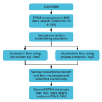
In today’s digital landscape, data security has become an indispensable feature for any data transfer protocol, including Peripheral Component Interconnect Express (PCIe). With the rising frequency and sophistication of digital attacks, ensuring data integrity, confidentiality, and authenticity during PCIe transport is crucial. To address these concerns, technologies like Security Protocol and Data Models (SPDM) have emerged as key enablers for secure communication. Component Measurement and Authentication (CMA) determines how SPDM is applied to PCIe systems. By employing these frameworks alongside advanced cryptographic techniques, such as elliptic curve cryptography (ECC), PCIe systems can safeguard sensitive data against potential threats. Siemens EDA recently published a whitepaper on this very topic.
CMA and SPDM: Foundations of PCIe Security
CMA and SPDM play a vital role in fortifying PCIe connections. Together, they establish secure sessions, authenticate communication endpoints, and facilitate encrypted data exchanges. SPDM achieves these goals by defining a series of messages that enable secure connections between devices. These messages negotiate protocol versions, advertise device capabilities, and determine supported cryptographic algorithms. Handshake secrets are generated using hash functions such as HMAC and HKDF, which are critical for encrypting and decrypting communication. After the successful exchange of SPDM requests, a secure session is established.
Symmetric vs. Asymmetric SPDM Flows
Symmetric Encryption: This method relies on a Pre-Shared Key (PSK) known to both parties before initiating communication. It is computationally efficient but requires secure key distribution beforehand.
Asymmetric Encryption: Public/private key pairs are used to eliminate the need for pre-shared keys. This approach enables stronger authentication mechanisms, such as digital signatures, ensuring that communication endpoints are verified.
SPDM supports both symmetric and asymmetric encryption flows to establish secure connections. While symmetric encryption is faster and less resource-intensive, asymmetric encryption provides superior security and solves key distribution challenges.
Key Generation and Authentication Techniques
Key generation is an essential part of the SPDM flow, with the Diffie-Hellman Key Exchange (DHE) algorithm playing a central role. The algorithm facilitates secure key exchanges by leveraging shared secrets generated during the handshake process.
Elliptic Curve Cryptography (ECC) enhances the DHE algorithm by performing complex operations on elliptic curves, enabling faster and more secure key generation. Authentication within SPDM is achieved through digital signatures, which validate the origin and integrity of transmitted data. By combining message hashing with encryption using a private key, digital signatures ensure that only authorized entities can participate in communication.
Advantages of Elliptic Curve Cryptography
Elliptic curve cryptography has gained prominence due to its ability to deliver equivalent security to traditional algorithms like RSA while requiring significantly smaller key sizes. This efficiency makes ECC particularly suited for resource-constrained environments like PCIe systems. For example, an ECC 256-bit key provides the same level of security as a 3072-bit RSA key, reducing computational overhead and improving performance. The smaller key sizes also simplify key management and accelerate cryptographic operations, making ECC an attractive choice for modern PCIe security.
Strengthening Security with ECC Algorithms
Elliptic curve cryptography further strengthens the security of PCIe transport by offering computational advantages over conventional methods. Its reliance on solving complex elliptic curve equations makes it resistant to cryptanalysis while reducing processing requirements. This efficiency allows for faster encryption and decryption, as well as quicker digital signature generation. Additionally, ECC’s smaller key sizes make it easier to maintain and manage cryptographic keys, ensuring seamless integration into PCIe systems.
Verification with Siemens VIP for PCIe
To ensure the successful implementation of CMA/SPDM, Siemens Verification IP (VIP) for PCIe provides a comprehensive framework for design verification. This solution is fully compliant with CMA Revision 1.1 and SPDM Version 1.3.0, offering robust testing capabilities for secure PCIe communication. Siemens VIP supports the generation of SPDM messages required to establish secure connections, along with APIs that enable flexible stimulus generation. Users can modify fields to create diverse test cases, covering both positive and negative scenarios.
Error injection and debugging are additional strengths of Siemens VIP, allowing designers to simulate fault conditions and analyze system behavior. The solution also supports both symmetric and asymmetric encryption flows, enabling a wide range of testing scenarios. Algorithms such as secp256r1 and secp384r1 are supported for Diffie-Hellman key generation, while digital signature algorithms like TPM_ALG_ECDSA_ECC_NIST_P256 ensure robust authentication. Moreover, Siemens VIP accommodates various device configurations, making it adaptable to the diverse capabilities advertised by different PCIe components.
Summary
CMA and SPDM provide a robust framework for PCIe security, enabling encrypted communication and authentication between devices. The integration of advanced cryptographic techniques, such as ECC, enhances these protocols by offering efficient and secure key generation, digital signatures, and encryption. Siemens Verification IP for PCIe ensures compliance with these security standards, offering extensive testing and debugging capabilities. Together, these technologies establish a new benchmark for PCIe transport security, protecting sensitive data against emerging threats in the digital age.
Tell us a little bit about yourself and your company.
Mahesh Tirupattur
I’m Mahesh Tirupattur. I’ve been with the company for over 20 years. Recently I took the role of CEO, where I drive business partnerships, IP licensing, and joint venture development. This change was a mutual decision between Alan Rogers and I. Alan wants to focus on technology innovation and he will be able to do that as President and CTO. I have a vision for taking the company to the next level and I will focus on that in my new role as CEO.
Analog Bits is truly a unique company. Through many customer and foundry partnerships we’ve become the leader at developing and delivering low-power integrated clocking, sensor and interconnect IP that are pervasive in virtually all of today’s semiconductors.
What was the most exciting high point of 2024 for your company?
This is a difficult one. There were many exciting achievements this past year, both with our foundry partners and our customers. If I had to pick one, I would say the introduction of advanced analog and mixed signal IP at cutting edge technologies. We presented proven results at 3nm, and we are moving to 2nm next.
For many years, analog IP was typically developed in older nodes. There have been many advances over the past few years that have changed this paradigm. Today, sensing and communication must be integrated on-chip with cutting edge technology. Analog Bits has met this challenge with a broad range of IP to address the needs of the latest AI and data center chip designs.
What was the biggest challenge your company faced in 2024?
The best way to describe this is a multi-dimensional balancing act. We need to deliver high-speed, high-precision IP that runs at the most advanced nodes with the lowest possible power. Achieving that combination requires a lot of analyses and tradeoffs.
How is your company’s work addressing this biggest challenge?
There are technical achievements that are certainly needed. For example, thermal considerations are top of mind for many design teams. To help with that we’ve developed a comprehensive on-die sensing IP portfolio. This technology helps to manage power, enhance reliability, and improve yield. Timing glitches are also becoming more prevalent in advanced designs. We also have a portfolio of glitch detection IP to address this growing problem. There are many more areas we cover, you get the idea.
But there is also an industry-level shift in thinking that is coming. For a long time, analog IP choices were made at the end of the design process. It was something of an afterthought to finish the design. I liken this to package design. For many years, the package for a monolithic chip was done near the end of the design to finish things up. With the growth of multi-die design, the package team is now an integral part of the system development team – the choices made impact and enable the entire project.
In the new multi-die environment, enabling IP that unlocks optimal power distribution, high-speed communication and eases thermal stress becomes a cornerstone item for system design. This is the IP that Analog Bits provides, and I am making changes to the company’s structure to allow us to be part of the system architecture team, ensuring all demands can be met early in the architectural definition phase. You will be hearing more details of how Analog Bits is moving upstream to address substantial challenges as early as possible.
What do you think the biggest growth area for 2025 will be, and why?
Thanks to the huge increase in data center expansion and AI application development, energy efficiency with superior performance and latency are an absolute requirement. To achieve these requirements, superior clocking, sensing, I/O and SerDes communication are all needed. This will be a big growth area, and these are all sweet spots for Analog Bits.
How is your company’s work addressing this growth?
Beyond design excellence, we focus on partnering with foundries and leading suppliers. A good example of this is the work we’ve done with Arm.
We worked on several integrated power management and clocking IPs with the company. Arm’s customers can readily use these solutions in N3P and soon in N2P. LDO regulator IPs were also part of the effort to efficiently manage the large absolute and dynamic current supplies to Arm CPU cores.
A case study of how CPU cores seamlessly integrate with Analog Bits LDO and Power Glitch Detector IPs, along with integrated clocking capabilities was presented at TSMC OIP in 2024. The implication of this work is substantial for advanced data center applications.
And our focus on working with system design teams early will clearly have a positive impact as well.
What conferences did you attend in 2024 and how was the traffic?
Beyond the usual industry trade shows such as DAC, Analog Bits supports many of the events of our foundry partners. We attend all the worldwide events for the TSMC Technology Symposium, TSMC OIP Ecosystem Forum, Samsung SAFE Forum, GlobalFoundries Technology Summit and Intel Foundry Services Direct Connect events. Each event brings us closer to key customers and our foundry partners, so we view them as all quite valuable.
Will you attend conferences in 2025? Same or more?
Each event we attended last year allowed us to reach an important segment of our customer base and partner network. I expect we will have a similar program this coming year. You can view the current plans on our website at https://www.analogbits.com/events/.
How do customers engage with your company?
As discussed, we are at a lot of shows. You can come by our booth, get the latest information and start a conversation with us. We also joined the Silicon Catalyst In-Kind Partner Ecosystem last year, so if you’re a startup in that incubator it’s easier to work with us. We also opened a new design center in Prague last year. You can also get things started by dropping a note to info@analogbits.com.
Additional questions or final comments?
2024 was a great year for Analog Bits and we’re excited to see the expansion on the horizon in 2025. If you’re working on advanced data center or AI applications, things just got a bit easier. If power management, performance or communication are challenges we can help.