By Jeff Wilson, Mentor Graphics
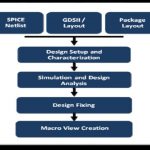
We’ve talked about the new requirements for Fill in IC design for advanced nodes in previous blogs on this site. This time I’d like describe the fill solution that Mentor and TSMC have jointly developed to meet the requirements of fill for TSMC’s 20nm (N20) manufacturing process.
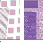
The traditional purpose for metal fill was to improve planarity in the chemical-mechanical polishing (or planarization) process. However, at advanced nodes fill is also used to manage effects related to electrochemical deposition (ECD), etch, lithography, stress, and rapid thermal annealing (RTA). TSMC’s N20 design rules require fill shapes to be evenly distributed and also require a greater variety of fill shapes (see figure). Designers need to add fill not just to metal layers, but also to poly, diffusion, and via layers. Other requirements of the newer technologies include analysis of density gradients, as well as absolute density. Additional constraints include perimeter and uniformity of fill spanning multiple layers. In many cases, multiple fill layers are interdependent.
Comparison of Front-End of Line (FEOL) fill at 65 nm and 20 nm. Fill shapes are no longer just squares, but now require support for multiple layers with a specific pattern to achieve higher density targets. (source: Mentor Graphics)
The collaborative solution from TSMC and Mentor for TSMC’s N20 fill requirements uses the Calibre® YieldEnhancer product’s SmartFill technology, which performs fill and analysis concurrently to ensure that the fill patterns meet TSMC’s forbidden pitch, multi-layer fill, and double patterning rules. Concurrent analysis of the layout also helps designers ensure that timing constraints are met by balancing the amount of fill against unwanted parasitic effects (i.e., added capacitance) as the fill process is being performed. The addition of double patterning (DP) at N20 also adds a new dimension to fill. Metal fill, like all the shapes in the layout, must be colored and decomposed into two masks. Fill observes DP rules to balance the light emitted through the mask to improve design uniformity.
Implementation of these requirements for 20nm required new technology development for SmartFill in the areas of core algorithms, support for multi-layer fill shapes and shape groupings, and repeatable cell-based fill patterns. The SmartFill solution uses the Calibre interfaces to integrate with full custom environments like Pyxis, Virtuoso, and Laker, and place and route tools such as Olympus-SoC, IC Compiler and Encounter to support net-aware fill. Designers can provide a list of critical nets that receive special treatment during the fill procedure and the filling engine can make informed fill placement decisions based on both the type of signals and which signals are timing-critical.
A key advantage of the SmartFill solution at TSMC is that it allows designers to meet IC fill constraints in a single pass with reduced impact on circuit performance and no manual intervention. The approach produces a relatively small post-fill GDS database size, which enables faster data transfers and quicker turnaround times, and the implementation fits into existing design flows to support final timing verification.
References
For more detail on the fill solution used at TSMC for 20nm, download the related white paper, “Advanced Filling Techniques for N20 and Beyond – SmartFill at TSMC.”
Author
Jeff Wilson is the DFM Product Marketing Manager in Mentor Graphics’ Calibre organization. He is responsible for the development of products that address the challenges of CMP and CAA. He previously worked at Motorola and SCS. Jeff received a BS in Design Engineering from Brigham Young University and an MBA from the University of Oregon.