It requires lateral thinking in bringing new innovation into conventional solutions to age-old hard problems. While the core logic design has evolved adding multiple functionalities onto a chip, now called SoC, the structural composition of DFT (Design for Testability) has remained more or less same based on XOR-based compression since long. Increasing SoC design sizes are pushing up increased test logic, tester time and test resources, thus increasing the test cost to the tune of billions of dollars. Alternatives to reduce such high test costs are awaited since long.
Typically shorter scan chains require lesser number of clock cycles to shift test bits and thus reduce test time, but that leads to far increased number of scan chains compared to the number of scan pins. This requires decompression logic between scan-in pins and the scan chains and at the other end compression logic between scan chains and scan-out pins; also the connections between scan chains and compression/decompression logic consumes significant routing resources. Increase in compression ratio (i.e. number of scan chains to number of scan pins) increases compression/decompression logic impacting the die size and routing resources. Also, higher compression ratio beyond certain limit can no more reduce the test time and can adversely impact on test coverage too.
Although about 100x compression ratio is seen optimal with current XOR architecture of compression logic, it consumes a significant ~4% of total chip routing; that increases to 10% if compression ratio is increased to 400x which outweighs the saving in test cost. Do we have alternatives to achieve higher compression ratio yet consume lesser routing resource and achieve higher test coverage?
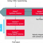
Here comes Cadencewith its new Modus[SUP]TM[/SUP] Test Solutionwith physically aware 2D Elastic Compression architecture integrated into Cadence digital flow. This innovative solution has several patents pending.
The Modus Test Solution is integrated with Cadence’s Genus[SUP]TM[/SUP]Physical Synthesis, Innovus[SUP]TM[/SUP]P&R system, and Tempus[SUP]TM[/SUP]Timing Signoff solution in a common environment to provide a seamless flow for digital designs which can achieve up to 2.6x lesser routing for compression logic and up to 3x lesser test time with the new 2D elastic compression technology compared to conventional 1D XOR-based compression logic.
To know more details about this new dimension in test compression, I had a nice opportunity talking to Paul Cunningham, VP R&D at Cadence, responsible for front-end digital design solution; earlier Paul was co-founder and CEO of Azuro which was acquired by Cadence in 2011.
In the 2D compression architecture, the compression logic forms a 2D grid across the chip. This allows the routing between the compression logic and the scan chains to be distributed evenly on the grid, thus requiring lesser wire lengths. With 2D compression, various types of designs including CPU, GPU, Networking, DSP and Automotive chips in the range of 1.3 to 2.5 million instances require same wire length at 400x compression ratio as compared to that at 100x compression ratio with traditional 1D XOR compression.
Another innovation added to the compression technology is to add elasticity by embedding registers and feedback loops in the decompression logic. This allows controlling care bits sequentially across multiple scan cycles during ATPG (Automatic Test Pattern Generation), thus maintaining fault coverage at high levels. With 2D elastic compression, compression ratios beyond 400x can be easily achieved without loss of fault coverage. And test time can be reduced by up to 3x compared to that with traditional 1D XOR compression. The designs discussed above have shown test time saving in the range of 1.6x to 3.6x, all with fault coverage > 99%; a little more than that achieved with 1D XOR compression.
Also, the Modus Test Solution allows automatic insertion of a single shared test access bus to enable one MBIST controller to service multiple memories, thus separating CPU for higher performance.
Cadence Modus Test Solution provides complete test features for scan, MBIST, logic BIST, ATPG, and self diagnostics in a common environment with synthesis, implementation, and timing signoff including debugging and scripting.
This new innovation in test solution for SoCs is a solid opportunity for Cadence to improve their market share in test automation business, currently dominated by Mentor’s TestKompress. There are good customer endorsements on this technology which can be seen in Cadence’s press release on Modus Test Solution HERE.
Pawan Kumar Fangaria
Founder & President at www.fangarias.com