Secure-IC at DAC 2025: Building Trust into Tomorrow’s Chips and Systems
As semiconductor innovation accelerates, the chiplet-based design paradigm is redefining the landscape of advanced electronic systems. At DAC 2025, Secure-IC (booth #1208) will present a comprehensive suite of technologies engineered to address the security challenges arising from this evolution—highlighting scalable solutions for secure chiplet integration, Post-Quantum Cryptography, MACsec IP for secure automotive and infrastructure Ethernet, and cybersecurity-by-design methodologies.
Securing the Chiplet Revolution
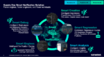
With the increasing disaggregation of SoCs into modular chiplets within a System-in-Package (SiP), the need for secure interoperability becomes critical. At the heart of Secure-IC’s offering is the Securyzr™ iSE s500 neo, a hardware Root of Trust (RoT) tailored for multi-die architectures. Designed to secure inter-chiplet communication and lifecycle management, it supports key security services like chiplet hardware and software bill-of-materials (HBOM/SBOM) verification, remote attestation, and cryptographic isolation.
This architecture will be explored in depth during the DAC 2025 session titled “Securing Chiplet Integration: A System-in-Package Security Architecture“ (Monday, June 23, 3:30pm PDT), co-presented by Secure-IC’s Sylvain Guilley and Cadence’s Junie Um. The talk outlines a protection profile framework to formalize security requirements across the chiplet lifecycle—from enrollment and key provisioning to post-quantum key renewal.
MACsec IP high-speed and automotive-grade
Secure-IC’s MACsec IP solution further extends the company’s portfolio by delivering robust, silicon-proven communication security. Validated with Cadence VIP, the IP achieves throughput scaling up to 1.6 Tbps, positioning it as a ready-to-integrate solution for next-generation automotive and infrastructure-grade systems.
Designed with automotive compliance in mind, the MACsec IP supports AES-GCM 256-bit encryption, ISO 26262 (ASIL-B), and enables secure high-speed links between ECUs, domain controllers, and central compute nodes. The fully integrated stack—MAC, MACsec, and Cadence PHY—provides a streamlined approach for designers to embed trusted hardware communication into their systems.
System-Level Security and Certification Support
Secure-IC’s Securyzr™ platform spans from embedded RoTs to software and cloud-based monitoring, offering full-stack protection. Beyond silicon, the platform includes standardized software interfaces, security lifecycle management, and services that simplify certification under frameworks like SESIP, PSA Certified, Common Criteria, and ISO 26262.
This integrated approach ensures that security is not just a hardware feature, but an architectural foundation—supporting developers from pre-silicon design to compliance and deployment.
Preparing for the Post-Quantum Era
The growing urgency to protect systems against future quantum threats is also addressed through Secure-IC’s PQC-ready solutions. Featuring CAVP-certified PQC algorithms, these technologies provide a pathway to quantum-resilient designs, ensuring long-term data protection and compliance with emerging standards.
Security Verification in the Design Flow
To reinforce security at the earliest stages of development, Secure-IC’s toolchain includes Catalyzr™ and Virtualyzr™. These solutions enable vulnerability analysis, virtual fault injection, and simulation-based verification—empowering design teams to evaluate physical attack resistance and compliance from day one.
Visit Secure-IC at DAC 2025 (Booth #1208) to explore how its cutting-edge technologies are securing the next generation of chiplets and connected systems.
Learn more or book a meeting with Secure-IC at DAC >>
Also Read:
Anirudh Keynote at CadenceLIVE 2025 Reveals Millennium M2000
Certification for Post-Quantum Cryptography gaining momentum