Building devices for the IoT has become especially challenging thanks to two conflicting requirements. The device has to be small and ultra-low power in most applications but also in many of those applications it has to provide a high-level of security, especially to defend high-value targets like smart metering, payment terminals, embedded SIM cards and mobile and wearable payment systems. There was a fantasy for a while that security heavy-lifting could be handed off to the cloud, but that idea died a quick death when we realized that remote security comes with significant latency problems, man-in-the-middle exposure and potentially worse power implications than you would find in local security.
But while local security consumes less power than a remote option, it consumes more power than no security. So when you’re trying to prove you have the least power-hungry yet still secure solution, differences in PPA profiles between different security solutions really matter.
We should also understand that many IoT devices are deployed with an expectation of long lifetimes and needing at most infrequent physical monitoring. Therefore attackers can, with little personal risk, install equipment around a device to inject faults, jiggle the power supply or use light (on a decapped device) to jiggle state elements, and they can steal keys by monitoring bus activity or even extract high-value keys through side-channel analysis on power rail variations, instruction timing or EMI emissions.
Traditional software vectors for attack will also be popular since these low-power devices cannot afford traditional software defenses, so malware exploiting well known weaknesses like buffer overflows can potentially inject itself into privileged operation modes or other opportunities for tampering.
But attacking a single device is generally not going to be the end goal. The big payback for an attacker is to find an exploit which can be reused on many targets. This is where security through diversity is an important part of a system-wide defense and where, I believe, there may be an unexpected weakness in over-reliance on a dominant CPU architecture. Interesting targets for hackers have to promise significant financial return or at least significant bragging rights in hacker circles. A successful exploit which can only compromise a limited number of targets offers neither. Which doesn’t rule out the possibility of an attack, but it does make you a much less interesting target.
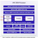
The Synopsys ARC SEM architecture offers solutions to address each of these needs. First, the architecture itself leads in PPA in the industry. So you start with an ultra-low-power solution which also has built-in security.
The architecture provides multiple defenses against attack, some well-known, others quite intriguing for support of security through diversity, even between devices. In this latter class, while ARC is already well-established in support functions like audio and video in mobile apps, in home automation and in automotive and disk controllers, Synopsys acknowledges that it’s not the market leader in embedded CPUs. But that position puts them lower on the priority list for attacks – see above.
Second, the ARC processor extension technology (APEX) helps a chip-maker further increase diversity. Custom instructions added to the base set further complicate attacks like differential analysis because the instruction-set reference is no longer completely accessible. And third the pipeline is very tamper-resistant because instruction and data are read encrypted from memory, using scrambled addresses; these are unscrambled/unencrypted in-flight for computation and are never stored in plaintext. The development team have control over this process, and can even make it differ even from device to device.
Other defenses include support for uniform instruction timing and timing and power randomization, for defense against side-channel attacks. (Synopsys also offers a CryptoPack solution for cryptography algorithms using these features.) If you need JTAG access, they offer a challenge/response mechanism to support a secure JTAG option, though I expect most would advise fusing access through that port before shipping. The SEM core provides a secure memory protection unit supporting 16 regions, with per region scrambling and encryption.
The ARC SEM processor offers these and other security functions and interfaces for a comprehensive security solution on which you can build a full-featured Trusted Execution Environment. Software control is managed through SecureShield, which provides control of privilege levels, memory region access and scrambling/encryption in the pipeline, and secure peripheral and IP access, these together being managed at the OS level through a microvisor to support the creation and management of containers.
Still, you may think “why not just use a better-known solution?”. The first part of the answer has to be power. If you need the lowest power solution, you have to go with the CPU that meets that objective, while also offering strong security, independent of the supplier. Market adoption isn’t a problem – there are plenty of ARC-based systems in production. The SEM core builds on that proven platform, and if you know anything about Synopsys, you know they are not fans of research projects. They told me they saw customer demand to address gaps in the market, for legacy microcontroller-based solutions needing upgrade with an emphasis on ultra-low power and security in a small form-factor, also for emerging applications with similar needs. In both cases, the ARC SEM processor is targeted to address tradeoffs between technical and market needs where a default processor choice doesn’t necessarily fit well.
Finally, give a thought to that diversity topic. If a clever hacker figures out a way into a smart meter, are you sure that payments systems, machine controls and grid management will never be at immediate risk from the same attack? There are some interesting differentiation possibilities in being able to say your security systems don’t share DNA with competitive solutions so are intrinsically firewalled from attacks on mainstream CPU platforms (and also from attacks on systems based on similar but tweaked DNA). You can learn more about the complete Synopsys ARC Processor family by clicking HERE.