For an industry that drives improvement at an exponential rate it is funny how often something old is new again. Intel went into high volume production on 22nm in 2011, and TSMC and Samsung have both had 20nm technologies in production for several years. And yet, recently we have seen renewed interest in 22nm. GLOBALFOUNDRIES has a 22nm FDSOI technology (22FDX) ramping now, at their recent technology forum TSMC announced a bulk 22nm technology 22ULP for 2017 production and this week Intel also announced a new 22nm FinFET technology 22FFL or 2017 production. Why the resurgence of interest in 22nm?
20nm/22nm is the last node where the industry primarily relied on planar bulk technology and is also the break point where multi-patterning starts to come in. At smaller dimensions’ leakage issues have driven the transition to fully depleted devices with FinFETs leading the way. FinFETs provide excellent drive current and a good scaling path with 16nm/14nm processes in high volume production, 10nm ramping and 7nm on the horizon. With each new node, the cost to manufacture a transistor has come down and Moore’s law has continued, but this has come at a high price. Design rules have been growing rapidly and the cost to design on these processes is so high that only the largest volume products can justify the necessary investment in development costs. With each new node, fewer products will be designed onto each new technology. One of the key emerging areas for the industry is IOT where the opportunity space is expected to be split between many lower volume products. The need for processes with lower design costs is obvious. IOT we will also need very low power, RF, analog and reasonable digital density. All of the three companies mentioned above are targeting this market with these new 22nm processes.
The key 22nm process objectives are low design cost, little or no multi-patterning, low power and the features needed for IOT and mobile.
GLOBALFOUNDRIES (GF) 22FDX
I have written about 22FDX previously here and here. 22FDX is based on fully depleted SOI (FDSOI) and offers the unique ability to use biasing to achieve multiple threshold voltages and dynamically scale performance. 22FDX offers the lowest operating voltage of any process I am aware of at 0.4 volts. Since power consumption is proportional to voltage squared, 22FDX should provide very low power operation. 22FDX offers 50% faster speed or 18% lower power than GLOBALFOUNDRIES 28nm process. 22FDX also offers excellent RF performance with NMOS FT/FMAX of 350/325GHz and PMOS FT/FMAX of 290/250GHz. This is likely far higher than either of the other 22nm processes, for example GF 14LPP FinFET process only achieves FMAX of ~150GHz. 22FDX is ramping up now.
TSMC 22ULP
Announced only a few weeks ago, 22ULP is due to ramp by the end of 2017. 22ULP is based on a bulk technology and TSMC claims the Ion/Ioff curve is identical to a “22nm FDSOI” technology. The operating voltage is 0.6 volts and the process is said to offer 15% higher performance or 35% lower leakage than TSMC’s 28nm process.
Intel 22FFL
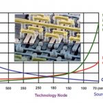
Announced this week, 22FFL is due to ramp in Q4 of 2017. 22FFL is based on Intel’s 22nm FinFET process that has been in production since 2011. 22FFL offers HP transistor with performance similar to Intel’s 14++ process and low leakage transistors with >100x lower leakage, see figure 1. RF is supported although FinFET RF performance is likely not nearly as good as FDSOI due to higher parasitic capacitances.
Figure 1. 22FFL Performance.
Process comparison
All three company’s processes are targeted at lower design costs and meeting the needs of IOT types of applications. Table 1 compares some of the key process characteristics for the three processes.
border=”1″ align=”center”
|-
| style=”width: 156px” | Company
| style=”width: 65px; text-align: center” | GF
| style=”width: 66px; text-align: center” | TSMC
| style=”width: 60px; text-align: center” | Intel
|-
| style=”width: 156px” | Process name
| style=”width: 65px; text-align: center” | 22FDX
| style=”width: 66px; text-align: center” | 22ULP
| style=”width: 60px; text-align: center” | 22FFL
|-
| style=”width: 156px” | Process type
| style=”width: 65px; text-align: center” | FDSOI
| style=”width: 66px; text-align: center” | Bulk
| style=”width: 60px; text-align: center” | FinFET
|-
| style=”width: 156px” | CPP (nm)
| style=”width: 65px; text-align: center” | 90 est
| style=”width: 66px; text-align: center” | 105 est
| style=”width: 60px; text-align: center” | 108
|-
| style=”width: 156px” | MMP (nm)
| style=”width: 65px; text-align: center” | 78 est
| style=”width: 66px; text-align: center” | 80 est
| style=”width: 60px; text-align: center” | 90
|-
| style=”width: 156px” | Tracks
| style=”width: 65px; text-align: center” | 8
| style=”width: 66px; text-align: center” | 7
| style=”width: 60px; text-align: center” | 7
|-
| style=”width: 156px” | CPP x MMP x Track (nm2)
| style=”width: 65px; text-align: center” | 56,160
| style=”width: 66px; text-align: center” | 58,800
| style=”width: 60px; text-align: center” | 68,040
|-
| style=”width: 156px” | Vdd (volts)
| style=”width: 65px; text-align: center” | 0.4
| style=”width: 66px; text-align: center” | 0.6
| style=”width: 60px; text-align: center” | NA
|-
Looking at the three processes the GF 22FDX process appears to likely have the densest logic (although we do not have exact numbers for GF and TSMC). 22FDX use 2 multi-patterning layers in the middle of line to drive tighter interconnect plus has the smallest projected contacted poly pitch. 22FDX will also likely have the best RF performance and active power consumption. On other performance and leakage metrics we don’t have enough data to draw any conclusions yet.
One critical factor in designing for any technology is the availability of IP. With TSMC’s 22ULP being a planar bulk shrink from 28nm they will likely have the richest IP offering providing the fastest deign path. At their manufacturing day Intel had a foundry panel including executives from Cadence, ARM and Synopsys and they are clearly working on that area but likely still playing catch up. I know GF is also putting a lot of emphasis on IP and the design environment but it isn’t clear to me how much traction they are getting.
Conclusion
Designers of IOT and other mobile devices now have three new 22nm processes to choose from. The three processes take very different approaches. GF’s 22FDX is the most radical departure from the main stream but also likely delivers the best density, RF and power performance. TSMC’s 22ULP bulk planar process can likely offer the richest IP environment. Intel’s 22FFL is an evolution of the 22GP process that is one of the highest yielding processes in Intel’s history and offers 14++ like performance with very low leakage transistors.