The semiconductor manufacturing industry has hit a new era of data intensity. We know that we need to look at alternatives to silicon and that electrical interconnects are unable to keep pace. We know we need to design more chiplets and alter microchip architecture. But how much data are we talking specifically, and how much time do we have to readjust our analytics to keep pace with the tsunami of data that’s around the corner?
The industry’s response has been multifaceted. Advanced semiconductor design strategies, the adoption of chiplets, and the integration of optical I/O and photonics are enabling higher performance, faster AI computation, and increased modularity. These approaches overcome traditional electrical I/O limits and scale functionality across larger, heterogeneous systems. Yet these same innovations generate massive amounts of data, from design simulations to fab telemetry and optical and electrical test results, creating an unprecedented amount of
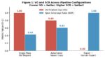
Measured per wafer, data volumes have already grown dramatically. Modern fabs with high-frequency sensors, inline inspection, multi-stage electrical testing, and optical characterization tools produce tens of terabytes per day. Compared to 2010, this is roughly 100% growth, highlighting that traditional analytics approaches will increasingly struggle, particularly when integrating diverse datasets across advanced architectures.
Accommodating this growth already requires more precise and detailed data genealogy tracking, now multiply that need by four. Aggregating design and simulation, process development, fab telemetry, metrology and inspection, electrical test, packaging and assembly, and system-level performance shows total data projected to grow 400% or more by 2030. Optical interconnects and photonics add high-resolution measurement streams, further increasing the complexity of correlating test results with process and design variables.
These diverse datasets demand more than storage; they require cross-domain correlation and insight to guide yield, reliability, throughput, and enable quick and precise root cause analytics.
Preparing for the Data Surge: Practical Steps for Engineers
Unified Data Infrastructure — Consolidate heterogeneous datasets across design, fab, metrology, and test environments while normalizing formats and maintaining consistent identifiers across wafers, die, and modules.
Commonality Correlation — Link design simulations, fab telemetry, metrology and inspection data, electrical test results, and optical characterization through shared identifiers to enable correlation across process, design, and performance variables.
Scalable Analytics Workflows — Implement batch or streaming pipelines capable of processing terabyte-scale datasets using distributed frameworks while supporting statistical, spatial, and pattern-based analysis across diverse data formats.
Data Genealogy and Lineage Management — Maintain traceability across design revisions, wafer fabrication, assembly, packaging, and system-level testing to enable faster root-cause analysis and yield optimization.
Operational Insight — Deliver engineering dashboards and automated alerts through tools such as Power BI, enabling faster decision-making across design, manufacturing, and quality teams.
Conclusion
The wave of data approaching semiconductor manufacturing is immense and multifaceted. While per-wafer manufacturing data may double, combined lifecycle datasets, including chiplets, packaging, and optical I/O, are projected to increase fourfold or more by 2030. Preparing now, by building unified, scalable analytics capable of transforming raw data into insight, is essential. Only then can manufacturers harness the benefits of chiplets, advanced design, and photonics without being overwhelmed by the digital tsunami they generate.
Fortunately, tools already exist to help manufacturers harness and organize this rapidly expanding data landscape.
Join our upcoming webinar, Scaling Silicon Photonics and Co-Packaged Optics: A Practical Blueprint for Managing Manufacturing Data, where we will walk through practical approaches for building resilient data infrastructure and analytics workflows for next-generation semiconductor systems.
Also Read:
CEO Interview with Aftkhar Aslam of yieldWerx
Qnity and Silicon Catalyst Light a Path to Success at the Chiplet Summit
Intel Foundry: How They Got Here and Scenarios for Improvement