Key Takeaways
- Diamond Quanta is bringing diamond out of the lab and into manufacturable devices today — converting decades of promise into practical impact for semiconductors, optics, and quantum. What was once thought ‘unavailable’ is becoming inevitable.
- The company’s platform centers on proprietary doping and annealing methods that enable both n- and p-type behavior in diamond, supporting real devices (diodes, FETs, and quantum emitters).
- Early collaborations with industry and research partners focus on high-temperature, high-voltage operation and reliability, targeting use in aerospace/defense, energy, and next-gen computing.
- At Diamond Quanta, we call this vision The Physics of Forever — unlocking the enduring properties of diamond to enable a new era of performance and reliability.
Adam Khan is a vanguard in diamond semiconductor technology, celebrated for his foresight and expertise in the industry. As the founder of AKHAN Semiconductor, he was instrumental in innovating lab-grown diamond thin-films for a myriad of applications, from enhancing the durability of smartphone screens and lenses with Miraj Diamond Glass® to bolstering the survivability of aircraft with Miraj Diamond Optics®.
Tell us about your company.
Diamond Quanta is pioneering engineered diamond as a practical semiconductor and quantum material platform.
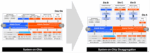
Our team combines decades of proprietary diamond growth and processing expertise with business development, IP strategy, and financial leadership. Our founders have committed capital and sweat equity, reflecting grit and full-time commitment. The goal: deliver devices that run cooler, last longer, and perform in places silicon, SiC, and GaN struggle—think high temperature, high field, high radiation, and high frequency environments. We’re building a platform that spans power electronics (diodes and FETs), quantum photonic sources, and ruggedized optical/sensor components. This platform embodies The Physics of Forever — our mission to make engineered diamond the foundation for the next era of electronics, optics, and quantum technologies, with physics-informed machine learning (ML) accelerating breakthroughs.
What problems are you solving?
Modern power and sensor systems are hitting thermal and reliability walls. Wide-bandgap incumbents have extended performance, but at the highest voltages, temperatures, and power densities, margins are thin. Diamond’s unique properties — a combination of ultra-wide bandgap, thermal conductivity, breakdown field, and carrier velocity — offer new headroom. Our focus is manufacturable doping and activation, so diamond can move from materials promise to device reality. For customers, this translates into significant economic value: up to 70% BOM savings, better reliability, and reduced cooling/qualification costs. In practice, this means up to 50% fewer cooling components are required in system designs, directly reducing weight, complexity, and cost. This is why leading OEMs are already engaging with Diamond Quanta — the industry cannot afford to wait.
What application areas are your strongest?
Our beachhead is display coatings, proving manufacturability and customer pull with Tier-1 glass suppliers. Beyond this zero-step, three near-term areas are:
- Power electronics for aerospace/defense, energy, and mobility where high-temperature, high-voltage switches reduce size, weight, and cooling needs.
- Quantum photonics with diamond color centers that enable secure comms, sensing, and computing.
- Extreme-environment sensing and optics such as high-temp pressure/current sensors and radiation-hard windows.
What keeps your customers up at night?
Reliability at temperature, efficiency under brutal duty cycles, and qualification risk. Many are boxed in by thermal budgets, derating, and complex cooling. They want devices that survive heat and radiation with predictable lifetime models—and they want a path to volume without a science-project supply chain.
What does the competitive landscape look like and how do you differentiate?
We respect SiC and GaN—they unlocked a generation of power density. Our differentiation is the engineered diamond device stack: co-doping, activation/defect-management anneals, and physics-first modeling. This enables both n- and p-type device functionality at higher breakdown and hotter junction operation while remaining compatible with mainstream fab flows. Compared to SiC and GaN, diamond offers >2x thermal conductivity and 10x higher heat tolerance, which translates into fewer design trade-offs at scale. We also maintain a strong IP portfolio across doping, annealing, and device architectures. Given recent M&A in coatings and semiconductor materials, we see optics as a divestiture option and the broader platform as a strategic acquisition target.
What new features/technology are you working on?
We are advancing ion-implantation co-doping with pulsed-laser and high-temp anneals to minimize defect complexes while activating dopants. Prototypes include Schottky and PiN diodes, followed by FETs exploiting diamond’s breakdown and thermal transport. For optics and quantum, coatings serve as a zero-step proving manufacturability from the start. We are also engineering emitters and coupling structures to deliver brighter, more uniform quantum sources.
- Process integration: Ion-implantation-based co-doping with pulsed-laser and high-temperature anneals designed to minimize defect complexes while activating dopants.
- Device prototypes: Next-gen Schottky and PiN diodes, followed by FET topologies that exploit diamond’s breakdown and thermal transport.
- Quantum photonics: Engineered emitters and coupling structures targeting brighter, more uniform sources for integrated photonics.
How do customers normally engage with your company?
We run structured evaluation and co-development programs: NDAs and problem statements → sample/device evaluation or compact model sharing → joint reliability plans → pre-production pilots. For quantum photonics, we offer early-access engagements around emitter performance and packaging. For power, we collaborate on application-specific stress profiles and targets (voltage class, Tj, SOA, RDS(on)/VF, switching loss).
What results can you share today?
We’ve demonstrated device-relevant doping/activation and early diode behavior at temperatures where SiC and GaN derate. Independent labs and partners validated high electron mobility (>555 cm²/V·s), reduced defect scattering in co-doped diamond, as published in a peer-reviewed MRS Advances white paper (Feb. 2025).[1] Building on this validation, our customer engagements show how these advances translate into system economics: up to 70% BOM savings, improved reliability, and fewer cooling components.
What’s next?
Our focus is converting prototypes to qualified parts in a few focused voltage/current classes, expanding our foundry-friendly process modules, and broadening our partner ecosystem—from epi and substrates to packaging and test. The through-line is the same: engineered diamond devices that simplify thermal design and push performance per watt in regimes that matter.
How can interested teams engage?
If you’re wrestling with heat, reliability, or extreme environments in power or sensing—or need practical quantum photonic sources—let’s compare requirements and agree on a pilot plan. We bring the materials, process, and device stack; you bring the mission profile. We have active customer discovery and development engagements (i.e., 20+ MNDAs, 2 MoUs, and a JTEA / SOW). Join the wave — Diamond Quanta is moving fast from promise to product. Let’s define your pilot plan now and help shape the next era of performance. Be part of The Physics of Forever.
Why did you join Silicon Catalyst and what are your goals in their 24-month program?
We joined Silicon Catalyst because it represents What’s Next in semiconductors — a platform proven to help deep-tech startups move from breakthrough science to market adoption. For Diamond Quanta, it’s not about incubation, it’s about accelerating impact through a network of industry partners, investors, and mentors.
Our goals in the 24-month program are clear: validate our engineered diamond platform in customer systems, secure early design-ins with Tier-1 partners, and build the operational and investor readiness to scale from prototypes into production.
Silicon Catalyst amplifies our mission — The Physics of Forever — making diamond the enduring foundation for electronics, optics, and quantum technologies that last longer, run cooler, and redefine performance.
- Khan, A.H., Kim, T.S., “Advanced co-doping techniques for enhanced charge transport in diamond-based materials,” MRS Advances, Feb. 2025. https://doi.org/10.1557/s43580-025-01206-x
Also Read:
CEO Interview with Andrew Skafel of Edgewater Wireless
Cutting Through the Fog: Hype versus Reality in Emerging Technologies