You are currently viewing SemiWiki as a guest which gives you limited access to the site. To view blog comments and experience other SemiWiki features you must be a registered member. Registration is fast, simple, and absolutely free so please, join our community today!
It is well-known that semiconductor growth is driven by AI. That simple statement breaks down into many complex use cases, each with its own requirements and challenges. A webinar will be presented by Synopsys on October 23 that focuses on the specific requirements for one of the most popular use cases – AI at the edge. The speaker is very knowledgeable on the topic and will treat the audience to a comprehensive view of the many requirements to be considered for successful deployment of AI at the edge. I highly recommend you register for this important event. A link is coming but first let’s look a little closer at this webinar on IP design considerations for real-time edge AI systems.
The Presenter
Hezi Saar
The value of any webinar is heavily influenced by the presenter. In this case, it’s Hezi Saar, executive director of product line management for mobile, automotive, and consumer IP for the Synopsys Solutions Group. Hezi brings more than 20 years of experience in the semiconductor and embedded systems industries. He has been with Synopsys for almost 17 years. He has also been the Chair of the Board of Directors for the MIPI Alliance for over nine years. Before Synopsys, Hezi was involved in product marketing, product management and design at Actel, ISD/Winbond and RAD Data Communications.
Hezi is quite good at explaining complex topics in an easy-to-understand way. The 25-minite webinar will be followed by a Q&A session with questions from the audience. I’m sure Hezi will do a great job with those questions as well.
Some Webinar Topics
Hezi presents a broad overview of IP architecture and integration methodologies that support real-time AI workloads at the edge. Here are some other topics he discusses:
A useful historical perspective of how AI has driven semiconductor growth is presented. The trends associated with AI models are discussed – the focus is to provide more capacity with less resources. How the quality of small models for edge AI has increased is also reviewed. The motivations for moving from the cloud to the edge is another interesting topic. Power efficiency is critical here. Hezi presents data that shows power consumption can be up to 200X more efficient on the device (edge) vs. the cloud.
There are many drivers and many benefits associated with moving from the cloud to the edge. He points out that this is what’s driving the next innovation cycle as summarized by the diagram below.
Hezi then presents a very useful and informative overview of a broad range of smart and connected devices at the edge. He discusses the unique requirements for cost, performance, area and power for these cases.
Market data is also presented, showing edge Al device shipments for smartphones dominating, with smart speakers showing growth as well. There is a lot of very useful discussion around new opportunities and how to address consumer demands for cost-effective products. Considerations for model choices are discussed, along with an overview of how AI companion chips can help.
Hezi also explores the impact of multi-die approaches. This technology will help in some cases more than others.
To Learn More
I have touched on only a subset of the topics Hezi covers in this very informative webinar. If AI at the edge is in your plans, this webinar will provide substantial and valuable information. I highly recommend investing the time to attend. It will take less than an hour.
The webinar will be held Thursday, October 23, 2025, from 10:00 AM – 11:00 AM Pacific Daylight Time. You can reserve your spot at the event here. And that’s a summary of a webinar on IP design considerations for real-time edge AI systems.
Why should high frequency circuit designers consider stability early in the design process? Isn’t there enough to worry about just making the circuit function at the fundamental frequency?
Figure 1: The Winslow Probe in ADS allows you to derive many figures of merit in postprocess using equations, based on a single simulation.
In the past, Microwave Engineers used to solve stability problems in the lab, perhaps adding bypassing or loss in a strategic location to stabilize their circuits. Stability was viewed as too complicated to model or predict, and the problems were usually easy enough to solve in the lab anyway. But things are changing. Across the entire wireless communications industry, standards are moving higher in frequency and systems are getting more complex. Instability arises from a combination of gain and feedback. In today’s circuits, gain is higher due to increasing device fT’s, and feedback is more prevalent because features are more compact and resonate more easily with signals that have smaller wavelengths. At the same time, advanced packaging technologies make the internals of the circuit less accessible than in the past, meaning things are harder to fix after the fact in the lab, even with the most apt technicians.
To make circuits which meet the needs of modern communications systems, designers need to master stability by truly understanding the root causes of problems in the circuit before building a design. The problem: stability is a very complex topic. Most high frequency design engineers use only the classic K-factor to assess circuits, but this technique is based on assumptions which may not be valid for modern circuits. Besides, K-factor only applies to a two-port network at the external I/O’s, while the circuit inside could be very complex and hinder visibility from the outside. There are many alternative techniques in literature, but they are sometimes difficult to apply correctly, and furthermore it’s not clear which one is best for any given application.
This webinar will help designers understand how instabilities fundamentally arise in their circuit and illustrate how to troubleshoot and resolve these issues up front in the design process before manufacturing.
This requires not only an understanding of theory and classic techniques, but also a practical knowledge of how to apply these techniques efficiently using modern design tools. This paper starts by reviewing the theory, discussing concepts like loop gain, return difference, and driving point impedance, and then expands to build a framework for applying these techniques to modern circuit design. The key is to use a new probe, called the WS-Probe, which has recently become available in Keysight’s Advanced Design System (ADS), to derive the necessary stability measures quickly and efficiently. The probe allows application of multiple stability analysis techniques to the circuit post-simulation for both small and large signal analysis in a non-invasive manner. The goal will be to arrive at a simple, straightforward, rigorous and easy to apply process to determine whether or not your design is stable, and if not, how to go about fixing it. After attending this webinar, you’ll look at stability in an entirely different way and the circuits you design will reflect that.
Figure 2: EM Circuit Excitation in ADS and RF Pro allows you to visualize and fix feedback paths that cause instability.
Figure 3: The New Winslow stability margin, only available in Keysight RF Circuit Professional (Nexus), allows you quantitatively discern the level of stability for your circuit.
As semiconductor designs move below 7 nm, parasitic effects—resistance, capacitance and inductance—become major threats to IC performance and reliability, often hiding where netlist reviews cannot reach. Design teams need advanced visualization tools like heat maps, layer-based analysis and direct layout correlation to spot and fix these invisible problems fast. Using a structured, multi-level workflow and an integrated EDA tool environment helps teams cut debug time and boost first-pass silicon success.
Seeing what the netlist cannot reveal
“Why does the simulation say this will work, but the chip fails every time in silicon?” If you’ve ever asked this question after weeks of painstaking debug, you are not alone. For IC designers working at the bleeding edge—below 7 nm, in billions of transistors and stacked 3D structures—the hardest problems are often the ones you can’t see. Invisible enemies lurk in every layout: resistance, capacitance and inductance effects that don’t manifest in your schematic, but can dominate performance and threaten reliability.
Modern parasitic problems are no longer minor corrections—they are decisive factors. Once you are working at the 5 nm node, hidden parasitics can account for more than half of total signal delay, compared to just one-tenth at older process technologies. Industry analysis reveals the critical impact: parasitic-related failures in advanced silicon designs can cost development teams weeks of debugging effort per incident.
This is the reality driving innovative approaches to visualization and analysis that help engineers see what a netlist alone cannot. By putting “eyes” on parasitics, designers can finally move from educated guesswork to precise solutions.
The unseen challenge: How parasitics threaten design success
Parasitic effects are electrical interactions that arise from the physical realities of semiconductor fabrication—unintentional resistance, capacitance and inductance generated by routing, stacking and proximity of metal structures. These are not intrinsic parts of the schematic, but unwelcome guests within every layout.
Their impact grows exponentially with process scaling and architectural complexity. For example:
Differential pairs and high-speed signaling: PCIe, DDR and SerDes interfaces depend on perfectly matched signal paths. Even a small mismatch in parasitic capacitance—just 5%—can trigger significant bit errors or total link failures. Identifying and fixing these subtle imbalances can require weeks of repeated layout analysis.
RF and high-frequency circuits: Circuits operating above 20 GHz are exceedingly sensitive to parasitics, such as inductive resonances in ground connections that can degrade transceiver fidelity by 30% or more.
Complex 3D architectures: FinFET and GAAFET structures introduce multi-layer parasitic effects that aren’t visible in traditional 2D reviews, making timing closure a moving target.
As stakes grow, traditional netlist-only methods are insufficient. The question becomes: How can engineers visualize, analyze and target the real root causes of performance failure within billions of intricate layout elements?
Elevating parasitic analysis: Making the invisible visible
To meet these needs, modern design workflows are evolving towards more comprehensive visualization and analysis techniques. Instead of reviewing static reports or text-based netlists, engineers use graphical representations that illuminate problem areas, quantify their impact and correlate electrical anomalies directly to their physical structures. A basic net visualization is illustrated in figure 1.
Figure 1. Net-level visualization example. A circuit layout visualization showing two interconnect traces. The image demonstrates net-level visualization, isolating and highlighting a specific net for detailed inspection while other elements remain visible in context.Key capabilities in next-generation visualization environments include:
Heat maps: Intuitive color gradients instantly reveal high-resistance or high-capacitance hotspots.
Layer-based views: Designers can track parasitic paths across stacked metal and via layers, uncovering issues that escape 2D inspection.
Component-level highlighting: Engineers can pinpoint exactly which polygon or segment contributes to a problematic parasitic value, enabling precise fixes rather than broad re-designs.
Filtering and sorting: The ability to focus on specific nets, layers or parasitic types streamlines the hunt for critical contributors.
Direct layout correlation: Electrical values align with real physical structures, reducing the disconnect between simulation and manufacturing reality.
The value of visualization is not just in finding problems, but in reducing time and uncertainty. Broad overview capabilities combined with precise local analysis enable teams to move quickly from symptom to root cause—and from root cause to targeted solution.
Multi-level debugging: A hierarchical approach to effective analysis
Advanced parasitic workflows employ a structured, multi-level strategy, guiding users from global assessment to pinpoint measurements:
Global net analysis: Identify potentially problematic nets and regions across the entire chip.
Layer interaction review: Track how each net interacts with the multi-layer stack, uncovering inter-layer coupling or bottlenecks. Figure 2 shows an example layer-based view.
Component-level inspection: Isolate individual parasitic values and their exact physical locations.
Figure 2. Layer-based analysis example. Circuit layout diagram displaying NET A across several interconnected layers. A legend identifies layer types and shows how each contributes to overall net performance.This approach speeds up troubleshooting by allowing systematic narrowing—from thousands of possible causes to a handful of tangible fixes.
Categorizing and targeting parasitic impacts
A powerful parasitic analysis solution organizes extraction results into structured categories (figure 3) that reflect real physical properties:
Resistance and inductance sorted by layer, because these effects depend heavily on geometry and routing.
Coupling capacitance and mutual inductance categorized by net, aligning with how signals cross-talk and interact in densely packed circuits.
This enables designers to sort, filter and prioritize the highest-risk contributors. For example, sorting for maximum capacitance between nets on a SerDes channel highlights potential sources of bit errors faster than a manual scan through pages of raw numbers.
Mapping and modifying physical structures for performance gains
Visualization environments bridge the divide between electrical anomalies and their specific physical causes. By highlighting polygon segments that drive high resistance, as shown in figures 3 and 4, engineers can immediately spot bottlenecks, narrow traces or problematic vias.
Figure 3. Resistance layout highlighting. Interconnect trace with a segment highlighted in orange and labeled “R=0.78” to demonstrate resistance layout highlighting.Figure 4. Point-to-point resistance layout highlighting. Two interconnect traces; one marked with driver and receiver points. The path between them is highlighted to indicate point-to-point resistance for targeted inspection.Capabilities like interactive resistance calculators help designers measure and report values between chosen pins in the layout viewer, making iterative optimization faster and more precise. Reports generated from these measurements ensure traceability and streamline workflow.
For capacitance, visualizing exact segments responsible for coupling (figure 5) or intrinsic (figure 6) effects means improvements can be focused—such as modifying only the problem edge instead of rerouting the entire net.
Figure 5. Coupling capacitance visualization. Diagram showing two interconnects, NET A and NET B, with the coupling capacitance between them quantified and highlighted.)*Figure 6. Intrinsic capacitance visualization. Alttext: NET A with segments along its path highlighted to indicate intrinsic capacitance.
Color-driven detection: Heat maps reveal hotspots
Heat maps are a powerful tool for visually identifying and prioritizing parasitic issues. Color-coded gradients transform raw data into intuitive displays: red for problematic intensity, green or blue for optimal performance (figure 7).
Figure 7. Intrinsic capacitance heatmap visualization. Segments colored from red to yellow to blue, showing intrinsic capacitance levels along NET A and NET B.Designers can set thresholds to reflect design-specific sensitivity, ensuring that attention is focused where the stakes are highest—such as moderate coupling capacitance in high-speed I/O blocks.
Reporting and connectivity: Detailed insights for optimization
Efficiently optimizing net performance depends on access to structured information, not just raw extraction data. Report-driven approaches present the hierarchy, connectivity and physical attributes of every net, along with all associated devices, ports and layer usage (figure 8).
Figure 8. Detailed net information and analysis results. Block diagram showing structured net information, with branches for Devices, Layers and Ports.
Switching between hierarchical and flat views helps teams analyze both the design logic and implementation details, all linked directly with the layout.
Parasitic-aware simulation: Unifying analysis and validation
Bringing schematic probing and full parasitic analysis into a single environment removes traditional workflow barriers (figure 9). Designers can launch simulations that account for every extracted parasitic effect—directly from the schematic, with results correlated to both physical layout and electrical performance.
Figure 9. Unified environment extraction and simulation workflow. Diagram showing flow from schematic to probed schematic with added parasitic elements, advancing to simulation waveform.This integrated approach promotes faster project cycles, deeper collaboration between circuit and layout teams, and higher confidence in first-pass silicon results.
Siemens Calibre: Solving the challenge with industry-leading visualization
The visualization and analysis methodologies described above are brought to life in Siemens Calibre extraction and debug solutions. Leading-edge design teams worldwide rely on Calibre xRC, Calibre xACT and Calibre xACT 3D for performance-accurate parasitic extraction, backed by Calibre Interactive and Calibre RVE for advanced, user-friendly visualization.
Calibre’s multi-level approach delivers measurable gains: users report up to 50% reductions in parasitic debugging time, 35% improvements in first-pass silicon success and a 25% increase in critical path timing performance. Structured workflows start with broad overview and drill down to component-level fixes, leveraging heat maps, filtering, and direct layout correlation, all in a unified environment.
What sets Calibre apart is its deeply integrated environment: from schematic probing and parasitic extraction to simulation, every step is streamlined. Engineers can highlight specific nets, layers or physical structures, instantly visualize hotspots and generate automated reports for compliance or ongoing optimization. This combination of visualization, quantification and interaction empowers rapid debug and smarter design decisions.
For organizations designing high-speed interfaces, RF circuits or complex multi-layer SoCs, Calibre offers the flexibility to build custom workflows that emphasize capacitance mitigation, resistance targeting or specialized 3D analysis as needed. Its modular framework adapts to each project’s unique challenges, supporting continuous innovation as process nodes scale down and design architectures evolve.
Conclusion: Seeing the future of IC performance
In the relentless drive to smaller nodes and greater circuit complexity, invisible parasitic effects have become major roadblocks to performance, reliability and time-to-market. By adopting visualization-rich analysis and interactive debugging, IC design teams gain the clarity needed to see, understand and solve what traditional netlists alone never reveal.
The future of high-performance IC design depends on making the invisible visible—transforming data into actionable insight, and insight into proven results. With tools like Siemens Calibre leading the way, design teams can meet the challenge and realize the full potential of modern semiconductor innovation.
Ready to dive deeper into strategies for tackling hidden parasitic effects in advanced IC design?
Omar Elabd is a Product Engineer at Siemens EDA, supporting Calibre extraction products. Based in Cairo, Egypt, Omar is an honors graduate of The American University Cairo with a major in Electronics and Communication Engineering along with a minor in Business Administration. Omar specializes in developing customer-specific flows for Calibre extraction tools and focuses on expanding the edge of current technology to meet evolving industry demands. He can be reached at omar.elabd@siemens.com
Many years ago, not long after we first launched SpyGlass, I was looking around for new areas where we could apply static verification methods and was fortunate to meet Ralph Marlett, a guy (now friend) with extensive experience in DFT. Ralph joined us and went on to build the very capable SpyGlass DFT app. So capable that SpyGlass DFT is now integrated inside Synopsys’ TestMAX Advisor to check that your RTL is DFT-clean prior to test insertion. As a full block or system design stabilizes, you can use TestMAX Advisor technology to insert DFT structures and verify this modified RTL continues to meet test requirements following insertion. These post-insertion checks are also enabled though the SpyGlass technology. Static analysis proves to be incredibly important in shifting DFT verification left to avoid late-stage schedule surprises.
Modern DFT demands
Test today is much more complex that just scan-based test. We must still support scan but also boundary scan, memory built-in self-test (MBIST) and logic built-in self-test (LBIST). The BIST options are important for in-system testing and, especially now, for on-the-fly self-test in mission-critical applications like cars. In addition to meeting these needs, feeding test data and control and reading results back for scan test across many scan chains in the design must be handled through test compression and decompression logic.
In large SoCs test infrastructure is commonly built hierarchically, where scan chains, compression, MBIST, LBIST and other test logic roll up to test interfaces around IPs and subsystems, which in turn roll up to SoC-level interfaces. Together all this hierarchical test logic, plus connectivity with the functional elements that are being tested, becomes a very complex logic overlay on top of the mission mode system.
OK, a lot of work but you build it once and you’re ready, apart from some later stage fine-tuning? Not necessarily. Updates to the mission mode design, whether pre-implementation or late stage ECOs, commonly require updates to the DFT logic and connectivity.
DFT logic must be verified and regressed like any other logic. We already know that verifying mission mode functionality is very resource- and time-consuming. Using the same dynamic methods to verify DFT logic in addition to mission mode logic would explode schedules and resource demands. Further, dynamic testing can never prove that a path between two points does not exist (needs to be demonstrated in some connectivity checks), and formal methods are not effective at these circuit sizes. Some level of dynamic verification is still useful as a double-check but not as the main method.
Fortunately, DFT logic elements such as MBIST and JTAG controllers are pre-verified, so the great majority of verification can be reduced to a limited set of connectivity checks. These can be grouped into value propagation, path existence or non-existence, and conditional connectivity checks. Examples commonly include that for some specified test mode certain design nodes must be in a specified state or should not be tied off to a specified state, or that a sensitizable (or sensitized) path should exist or should not exist between certain nodes. These concepts can be extended further to test for conditional connectivity, for example that a pin should be tied to a certain state OR should be driven a certain kind of element.
In short, most of the DFT functionality and its interaction with mission mode functionality can be verified through static connectivity checks. Once appropriate checks are defined, verification regressions should run in times comparable to those for other static checks.
The TestMAX approach
Connectivity checks for TestMAX are steered through Tcl commands as you might expect. When I first saw sample constraints files in the Webinar demos they seemed rather complex but the webinar hosts (Kiran Vittal, Executive Director Product Management and Markets at Synopsys and fellow Atrenta alum) and Ayush Goyal (Sr. Staff R&D engineer at Synopsys) pointed out that the way the constraints are constructed can easily can be made design independent. No doubt such a constraints file would take some effort to setup the first time but then could be reused across many designs.
Here I’m sure I’m going to display how long it has been since I did anything of this nature, but I found the approach intriguing, somewhat similar in principle to SQL-like operations on a database. You build lists of objects for value tests or pairs of objects for path tests, and you define what is required or illegal in such cases. List building is based on name-matching (allowing wild cards). If designs stick to appropriate naming conventions (e.g. a PLL name contains PLL) then the constraints should work.
Conditional connectivity checks simply continue this theme. A first check might require a “1” on a certain class of nodes. Whatever cases fail this check are gathered in a second list and checked against another test, for example whether surviving nodes are driven by some node in a different list you have defined. And so on.
Easy enough to understand. On performance, Ayush added that he knows of a design with over a billion flat instance and 80 million or more flip-flops in which they were able to run connectivity checks between 100 billion pairs of nodes in less than a day. Dynamic verification would have no chance of competing with that performance or with completeness of test.
Good stuff. You can register to watch the webinar HERE.
Over the years design reuse methodology created a market for Semiconductor IP (SIP), now with formal techniques there’s a need for Assertion IP (AIP). Where each AIP is a reusable and configurable verification component used in hardware design to detect protocol and functional violations in a Design Under Test (DUT). LUBIS EDA is focused on formal services and tools, so I received an update on their approach to developing these AIPs and detecting corner-case bugs in high-risk IPs.
Before I jump into the details of the approach that LUBIS EDA uses, let’s first review how simulation-based verification differs from formal verification. With simulation an engineer is writing stimulus to cover all the known states of a design, hoping that the coverage is high enough. With formal verification the formal tool figures out all the possible paths from inputs to outputs within a design.
Simulation-based verification
Formal-based verification
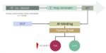
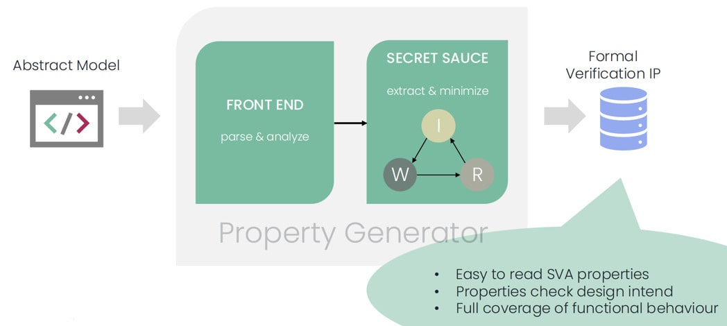
One approach used by LUBIS EDA is their in-house property generator, which works at the Electronic System Level (ESL) rather than Register Transfer Level (RTL). This enables them to deliver verification services that are faster, higher quality and more efficient. The property generator enables you to go from an abstract model to your AIP in a matter of minutes, which is a huge leap in verification productivity. Here’s what that flow looks like: first the abstract model is parsed and analyzed by the property generator, then the formal verification IP is created as System Verilog Assertions (SVA). These assertions check your design intent and provide full coverage of the functional behavior.
Property generator flow
Your abstract model at the ESL level is written in C++ or SystemC and can be simulated to verify its behavior, the Property Generator reads in that code and generates the AIP for you. The assertions are then bound to your RTL design through the refinement step which is supported by Large Language Models (LLMs) for a faster result. The assertions are human-readable and correct-by-construction, so you don’t need to have a dedicated assertion review session. Run your favorite formal tool in this flow and then look for any failures.
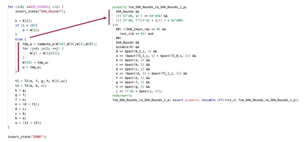
One example for applying this AIP approach is for cryptographic hash functions like SHA-512. The following shows the C++ model on the left and the property that is generated on the right that covers a portion of the model.
Summary
How does this approach make formal verification more efficient? Verification engineers can apply formal approaches by manually writing assertions. Manually writing formal assertions take time, error prone and requires expertise, so automating this step saves you engineering time and effort.
The generated Assertion IP (AIP) covers every possible scenario and stimuli to guarantee a bug-free design. This approach is also quite useful to help you verify blocks of logic or even complex IP cores.
Is your project under enormous time pressure and would you like to leverage the benefits of such an efficient approach? Then you should consider LUBIS EDA’s consulting services to achieve first-class SoC design quality. If you want to carry out your project yourself, there are also courses on formal verification that could help you work faster. LUBIS EDA’s website also has many useful blog articles on using formal verification techniques.
To take the next step, just contact the team at LUBIS EDA.
Cybersecurity is getting more critical every day. Thanks to sophisticated AI attacks, the need for hardware chip-level security is greater than ever. To fortify hardware against these types of attacks is not easy. There are three key attributes of a successful strategy: a well-designed root-of-trust, collaboration to ensure a well-integrated solution and conformance with the latest security standards. Secure-IC and Silicon Labs recently released a press announcement that had all of these attributes. The result is Secure-IC and Silicon Labs raise the bar for hardware security. Here are some of the details.
What Was Announced
It was announced that Secure-IC’s Securyzr™ neo Core Platform served as the Root of Trust (RoT) at the heart of the Series 3 Secure Vault subsystem, enabling Silicon Labs’ SiXG301 SoC to withstand advanced threats. There is a lot to unpack in that statement, so let’s look at some aspects of this new collaboration to understand its significance.
Why It’s Significant
PSA Certified is a global standard enabling trust in connected systems for the electronics industry. PSA stands for platform security architecture. The standard defines clear, easy-to-understand levels of robustness and assurance for the Root of Trust (RoT) in SoCs. These specifications can be used by OEMs and cloud service providers for example.
This effort started with experts from seven founding companies, SGS Brightsight, CAICT, Riscure Keysight, UL, Arm, security consultancy Prove & Run, and TrustCB, who acted as the certification body. Today, the scheme is managed by GlobalPlatform, ensuring its continued growth and alignment with global security needs.
There are four levels of security certification available from PSA, Level 4 being the newest and most comprehensive. According to PSA, it is intended for chip vendors who use an integrated Secure Enclave or external Secure Element that provides a high level of robustness to physical and software attacks. The diagram below, sourced from psacertified by GlobalPlatform, illustrates the development of these standards.
Evolution of PSA standards
Level 4 is targeted at fortifying against hardware attacks, including resilience against the most advanced physical threats. This specification aims to validate resilience against sophisticated physical attacks such as laser fault injection, side-channel analysis, micro probing, and voltage manipulation. So, this joint announcement blazes an important trail as the first design that conforms to this standard.
With billions of connected devices expected to enter the market in the coming years, PSA Level 4 certification provides assurance that Silicon Labs’ and Secure-IC’s solutions will remain resilient against evolving cyber and physical threats.
More Details
Secure-IC’s Securyzr neo Core Platform is designed to address the diverse embedded security needs of various industries and applications. From chip-level hardware security to comprehensive chip-to-cloud solutions, the platform offers tailored configurations to meet different market security requirements, standards and certifications. Backed by over a decade of development and deployment in various industries, this platform delivers unmatched performance and versatility for the most demanding applications. The S100 neo series is tailored for general IoT and connectivity. The figure below illustrates the breadth of markets that the platform supports.
Comments About the Announcement
Executives from both Secure-IC and Silicon Labs weighed in on this important announcement.
Daniel Cooley
Daniel Cooley, CTO and SVP at Silicon Labs commented, “Our collaboration with Secure-IC has been essential to pushing the boundaries of security in connected devices. By integrating Secure-IC’s Securyzr neo Core Platform as the Root of Trust in our Series 3 architecture, we achieved the world’s first PSA Level 4 certification, delivering unparalleled protection today while building the foundation to keep our customers secure against tomorrow’s evolving threats.”
Hassan Triqui
Hassan Triqui, CEO and Co-Founder of Secure-IC commented, “This certification underscores the maturity of our Securyzr neo Core Platform and the strength of our long-standing partnership with Silicon Labs. By uniting world-class embedded cybersecurity with Silicon Labs’ leadership in secure and energy-efficient IoT solutions, we are shaping the future of trusted connected devices and reinforcing our shared commitment to raising the bar for the entire industry.”
Synopsys recently held a webinar session on this topic and Gustavo Pimentel, Principal Product Marketing Manager at the company led the webinar session. Going into the webinar session, I found myself wondering: why focus on PCIe 5.0, eight years after its release? With the industry buzzing about Edge AI, cloud computing, and high-performance applications, it felt like talking about “old news.” That curiosity turned out to mirror some of the audience questions during the webinar Q&A session. Another common question was whether it made sense to skip PCIe 5.0 entirely and jump straight to PCIe 6.0.
Gustavo offered clear answers. He explained why, for most applications today, migrating from PCIe 4.0 to PCIe 5.0 is the practical path. PCIe 6.0 is only warranted if a customer’s application absolutely demands it. The discussion delved into both design techniques and architectural integration strategies, demonstrating how PCIe 5.0 remains a highly flexible solution for balancing power, performance, area and latency tradeoffs across industries.
Edge AI: Driving the Next Cycle of Innovation
Edge AI is no longer a futuristic concept—it’s driving real change across devices and data centers. By processing data closer to the source, it improves privacy, strengthens security, and delivers faster, more personalized user experiences, all while reducing reliance on the cloud. AI workloads themselves are growing at an unprecedented rate. Estimates suggest that by 2027–2028, about 50% of data center capacity will be AI-driven, up from 20% today. AI model sizes double roughly every four to six months, far outpacing Moore’s Law, and processing demands continue to escalate dramatically.
To efficiently handle this explosion of data, devices and systems need interconnects that can keep pace. PCIe 5.0, with its high bandwidth and low latency, is ideally suited to enable edge SoCs to process AI workloads efficiently, while maintaining strict power and area constraints. Its role is particularly critical in applications where latency, power, and space are all highly constrained, such as autonomous vehicles, mobile devices, and embedded AI systems.
Why PCIe 5.0 Remains Relevant
At 32 GT/s per lane, PCIe 5.0 doubles the bandwidth of PCIe 4.0 while remaining backward-compatible with previous generations. Its maturity and interoperability make it a dependable choice for designers navigating complex, high-performance systems. PCIe 5.0 serves a diverse range of applications, from high-performance computing and data centers to mobile multimedia, consumer devices, and automotive Edge AI.
For automotive systems, latency-sensitive workloads demand PCIe 5.0’s high throughput, while consumer electronics often prioritize minimizing footprint and power. In data centers and HPC environments, designers focus on maximizing bandwidth and efficiency. PCIe 5.0 provides the flexibility to achieve the optimal tradeoff in each case, making it a practical, future-ready solution.
Design and Low-Power Techniques
One of the key themes of the webinar was low-power design, essential for both edge devices and energy-efficient HPC systems. PCIe 5.0 includes power states like P1.2, which reduces energy usage while maintaining responsiveness, and P1.2PG, which uses dynamic power gating to further minimize consumption, albeit with slightly longer transitions to active operation.
Channel length also influences performance. Shorter chip-to-chip and card-to-card channels reduce latency and improve signal integrity, enabling devices to fully exploit PCIe 5.0’s high-speed capabilities. Migration strategies from PCIe 4.0 illustrate the flexibility offered by PCIe 5.0: designers can choose to increase bandwidth while keeping area and power nearly constant, or reduce lanes and beachfront size to save area and energy without sacrificing throughput. These design options allow PCIe 5.0 to meet the highly variable requirements of modern AI and computing workloads.
Integration Considerations for Edge SoCs
Incorporating PCIe 5.0 into edge SoCs requires careful planning around cost, time-to-market, reliability, and readiness. The webinar highlighted how integration strategies, alongside careful design techniques, allow PCIe 5.0 to support demanding workloads efficiently. By optimizing lane configuration, channel length, and power management, designers can create systems that balance high bandwidth, low latency, and power efficiency, tailored to specific application domains.
Adoption and Real-World Use
PCIe 5.0 adoption has progressed steadily. The automotive market, in particular, has ramped up faster than others, driven by latency-critical AI workloads and strict reliability requirements. By the end of 2022, PCIe 5.0 was widely deployed in automotive applications. In high-performance computing, standard PCIe 5.0 continues to deliver maximum throughput, while low-power, short-reach variants are increasingly common in edge and embedded devices. Production-proven IP solutions, such as those from Synopsys, demonstrate broad interoperability and first-pass silicon success, proving that PCIe 5.0 is both mature and ready for next-generation AI applications.
Audience Questions: Key Insights
The Q&A session addressed several questions that clarified PCIe 5.0’s ongoing relevance. When asked why not skip directly to PCIe 6.0, the answer was clear: PCIe 6.0 requires major changes to PHYs and controllers, which increase area and power significantly. Adoption of PCIe 5.0 is already sufficient for the vast majority of use cases. Tradeoff decisions—whether to increase bandwidth while keeping area constant, or reduce area while maintaining bandwidth—depend entirely on the application. Standard PCIe 5.0 supports HPC workloads, while low-power, short-reach variants are increasingly deployed for edge and embedded systems.
Summary
PCIe 5.0 may have been released quite a few years ago, but it remains a critical enabler for Edge AI and high-performance applications. Its combination of maturity, interoperability, high bandwidth, and flexible design tradeoffs makes it a practical choice across markets, from automotive to consumer electronics and data centers. Far from being “old technology,” PCIe 5.0 allows designers to deliver high performance where it matters, while balancing power and area efficiently. For Edge AI, HPC, and embedded applications alike, PCIe 5.0 continues to be a versatile and reliable solution, helping to drive the next cycle of innovation.
Overview: Protecting ICs from costly ESD and latch-up failures
Electrostatic discharge (ESD) events cost the semiconductor industry an estimated $8 billion annually in lost productivity, warranty claims and product failures [1].
Ensuring the robust protection of integrated circuits (ICs) against various electrical phenomena, is a critical and often complex task in modern electronic design automation (EDA) verification, with even minor ESD incidents capable of triggering catastrophic latch-up events that can permanently damage sensitive components Preventing latch-up— a parasitic condition that can lead to device failure—is paramount, with guard rings playing a crucial role in its mitigation. ESD mitigation requires a multifaceted approach centered around robust guard ring implementation and comprehensive verification.
Different IC design companies employ diverse protection methodologies, design flows and verification tools, leading to potential inconsistencies. To establish a consistent, comprehensive and efficient verification flow for critical reliability aspects, the ESD Association (ESDA) provides recommended compliance checks. The Calibre PERC reliability platform from Siemens Digital Industries Software offers a suite of easy-to-use, pre-coded packaged checks for latch-up and the effective implementation of guard rings. This allows design companies to perform fast and efficient verification of ESD protections without the need to develop and maintain their own custom checks. By streamlining the design process. Calibre PERC helps design teams enhance overall device reliability. [4]
The pervasive threat of electrostatic discharge (ESD)
Electrostatic Discharge (ESD) is a rapid, uncontrolled transfer of static electricity between two objects at different electrical potentials. This static charge can accumulate on various surfaces or even human bodies through friction or induction. When a charged object comes into proximity or direct contact with a less charged or grounded object, the stored electrical energy discharges instantaneously, often generating thousands of volts and significant current pulses lasting only nanoseconds.
While static shocks are familiar phenomenon, in advanced manufacturing and electronic environments, ESD events pose a severe and costly threat. Even minor discharges can inflict critical damage on highly sensitive IC components. This damage can manifest in several ways:
Immediate catastrophic failure, where the device ceases to function
Latent damage, which may not cause immediate malfunction but degrades performance over time, leading to premature field failures
Parametric shifts, altering device characteristics without complete failure
Common failure mechanisms include gate oxide breakdown due to high electric fields, junction damage from excessive current and metallization burnout caused by localized heating. Such incidents directly translate into reduced manufacturing yields, increased warranty claims, costly product recalls, and significant financial losses for semiconductor companies. [3,6]
The challenges of latch-up
Complementing ESD as a paramount reliability concern in IC design is the phenomenon of latch-up. Latch-up refers to the inadvertent triggering of a parasitic Silicon Controlled Rectifier (SCR) structure inherent within the bulk CMOS (Complementary Metal-Oxide-Semiconductor) process. This parasitic SCR is formed by the interaction of adjacent p-n junctions, specifically the p-well, n-well, and substrate, creating a parasitic NPN-PNP bipolar transistor pair.
Under certain conditions, such as voltage transients, overvoltage events or current injection into input/output (I/O) pins, this parasitic SCR can be triggered into a low-impedance, high-current state. Once triggered, a positive feedback loop is established between the parasitic bipolar transistors, sustaining a large, uncontrolled current flow between the power supply and ground.
This sustained high current draw can lead to several severe consequences:
Complete functional failure of the circuit
Thermal runaway due to excessive heat generation
Permanent physical damage to the device (e.g., metal trace burnout, junction degradation)
Collapse of the system’s power supply.
Latch-up events can be initiated by various factors, including I/O overvoltage, power supply transients, or even an ESD event that injects sufficient current to trigger the parasitic structure. Once latch-up occurs, it is challenging to mitigate and typically requires the device to be powered off or physically reset to restore normal operation, highlighting the critical need for robust prevention mechanisms during the design phase.
Figure 1. The components of a latch-up event.
Latch-up prevention techniques
Latch-up prevention is a critical aspect of integrated circuit (IC) design, employing a multifaceted approach to mitigate the risks associated with parasitic current flow.
A cornerstone of latch-up prevention is the careful optimization of the IC layout. This involves strategic placement and spacing of components to inherently suppress the formation of parasitic thyristors—the PNPN structures responsible for latch-up. Central to this strategy is the implementation of guard rings—heavily doped regions strategically placed around sensitive transistors and circuit blocks.
Guard rings serve two key functions:
They absorb minority carriers, preventing them from reaching and activating the parasitic bipolar transistors that constitute the latch-up path.
They act as physical barriers, diverting excess current away from vulnerable areas and providing electrical isolation between different regions of the IC. [2]
This helps minimize unwanted interactions, maintain signal integrity, and enhance overall IC robustness by containing and dissipating potential trigger currents.
Beyond guard rings, other critical latch-up prevention techniques include:
Maintaining optimal spacing between p-wells and n-wells to physically increase the resistance of parasitic paths
Employing precise biasing techniques to control the substrate potential and keep parasitic elements in a non-conductive state [2]
The integration of robust ESD protection circuits also plays an indirect role by clamping and shunting transient overvoltages and overcurrents that could otherwise trigger latch-up.
Finally, advanced semiconductor processing techniques, such as using Silicon-On-Insulator (SOI) technology, significantly enhance latch-up immunity by providing intrinsic dielectric isolation between devices, dramatically reducing parasitic interactions and virtually eliminating bulk latch-up paths. Similarly, precise optimization of doping concentrations and profiles within the silicon substrate allows for better control over the electrical characteristics of parasitic elements, making them less prone to activation.
By integrating these comprehensive design and process techniques, IC designers can significantly minimize the risk of latch-up events, ensuring the reliable performance of integrated circuits across a wide spectrum of applications.
ESDA’s reliability guidelines for IC designers
ESD Association (ESDA) is a leading industry association dedicated to advancing the understanding, theory and practice of electrostatic discharge (ESD) avoidance. Recognizing the critical impact of ESD on IC reliability, the ESDA develops and publishes comprehensive guidelines, standards, and technical reports. These resources provide a standardized framework of design rules and corresponding compliance checks, serving as indispensable tools for both the electronic design automation (EDA) industry and the ESD design community. Their primary aim is to empower IC design teams to proactively protect their layouts from the damaging effects of ESD events and ensure overall device robustness. [2,3]
ESDA latch-up guard rings checks
Building upon these industry standards, EDA vendors strive to develop advanced verification solutions to address these critical reliability concerns. An example of such a solution is the Calibre PERC reliability platform from Siemens Digital Industries Software. This platform is designed to perform a range of complex design verification checks and can be integrated into existing design flows. It supports verification at various levels, including cell, block, and full-chip, and facilitates the implementation of reliability checks using both standard rules provided by foundries and custom rules defined by design teams.[5]
To effectively address these pervasive reliability threats, all potential sources of ESD and latch-up events within an IC design must be thoroughly evaluated and verified. In this context, Calibre PERC specifically addresses latch-up prevention by incorporating latch-up guard rings packaged check. This check support various critical verification aspects, encompassing 14 distinct checks, shown in figure 2, further categorized into five key areas:
Check guard ring existence
Check guard ring width
Check max spacing between Guard rings
Check victims in aggressor’s danger zone
Check guard rings connectivity
Figure 2. Latch-up guard rings checks.
By enabling the early identification and resolution of potential latch-up issues during the design phase, these advanced checks significantly reduce time-to-market for microelectronics designers and producers. This proactive approach prevents costly post-production failures, thereby improving yield, enhancing device reliability and compliance, minimizing field failures, and streamlining design iterations for faster, more efficient product development.
Guard rings existence checks
Verifying the existence of guard rings in a design is critical because these structures serve as a primary protective measure against latch-up phenomena in CMOS and mixed-signal circuits. Guard rings act as barriers that prevent injected minority carriers—generated during transient events, such as voltage spikes or substrate noise—from reaching sensitive device junctions and triggering parasitic thyristor paths. Without the presence of guard rings, the circuit is left exposed to increased risk of latch-up, which can lead to excessive current flow, functional failure, or even permanent damage. Therefore, confirming that guard rings are present wherever needed ensures that the foundational layer of latch-up protection is robustly in place. These rules verify the existence of the four types of guard rings (GR) illustrated in figure 3. The checks ensure that:
1st P type GR must enclose N+ aggressor
1st N type GR must enclose P+ aggressor
2nd P type GR must enclose P+ aggressor
2nd N type GR must enclose N+ aggressor
Guard rings’ width checks
The width of a guard ring strongly influences its ability to intercept and collect stray charge carriers before they reach vulnerable regions of the integrated circuit. If the guard ring is too narrow, it may not fully encompass the region it is supposed to protect, allowing some injected carriers to bypass the barrier and trigger latch-up. Adequate ring width ensures a greater area for carrier collection and improves the effectiveness of the ring as a protective shield. By rigorously checking that guard ring widths adhere to design rules and process requirements, engineers can significantly reduce the risk of latch-up and enhance the reliability and longevity of the chip.
The checks cover:
Width of P type Guard rings
Width of N type Guard rings
Guard rings spacing checks
The spacing between adjacent guard rings and aggressors plays a vital role in maintaining continuous protection across the chip. If guard rings are spaced too far apart, gaps appear in the protective network, leaving certain regions susceptible to carrier migration and latch-up initiation. Carefully monitoring and enforcing the maximum allowable spacing ensures full coverage of critical areas, creating a seamless defense system that blocks potential latch-up pathways. These checks help eliminate weak points in the design and boosts overall device robustness by maintaining the integrity of the guard ring network.
The checks cover:
max spacing between P type aggressor and 1st N type guard ring
max spacing between 1st N type guard ring and 2nd P type guard ring
max spacing between N type aggressor and 1st P type guard ring
max spacing between 1st P type guard ring and 2nd N type guard ring
Aggressor’s danger zone checks
Sensitive components, referred to as “victims,” located near regions with high-current drive or frequent switching activities—known as “aggressors”—are at particular risk for latch-up. In these danger zones, increased noise and carrier injection elevate the probability of parasitic conduction. By identifying and analyzing potential victims within these aggressive regions, engineers can prioritize additional guard ring protection and optimize layout strategies to mitigate risk. This targeted approach greatly enhances the effectiveness of latch-up prevention by focusing resources and attention on the most vulnerable spots within the circuit by check the non-protected victims in an aggressor’s danger zone, where the danger zone is marked by drawing a radius around the aggressors, as illustrated in figure 4.
The checks cover:
max spacing between P type aggressor and 1st N type guard ring
max spacing between 1st N type guard ring and 2nd P type guard
Figure 4. The victims in an aggressor’s danger zone.
Guard rings connectivity checks
Proper guard ring connectivity is essential to ensure that these protective structures are electrically functional and capable of steering excess charge to a safe potential, typically ground or VSS. If guard rings are not correctly tied to the designated bias, their ability to collect and divert injected carriers is compromised, undermining latch-up prevention. Connectivity checks involve confirming robust electrical contact and continuity through all relevant routes and layers. Ensuring reliable guard ring connections fortifies the overall defense against latch-up, preserving the operational integrity and safety of the integrated circuit throughout its lifecycle.
The checks cover:
N type Guard rings not connected to VDD.
P type Guard rings not connected to VSS
Simplifying ESD check implementation with packaged checks
However, the mere availability of ESDA checks is only the initial step; designers often face challenges in effectively setting up and executing these checks within their specific environments. To significantly simplify and standardize the application of ESDA guidelines, Electronic Design Automation (EDA) companies, such as Siemens EDA, encapsulate these checks into pre-coded, packaged solutions. These readily deployable checks can be seamlessly integrated into a design team’s existing reliability verification flow, eliminating the need for manually coded checks and the associated complexities. Designers can embed these Calibre PERC reliability checks directly into their current design flows, leveraging the integrated Calibre platform for comprehensive cell, block, and full-chip verification. This approach, which brings together rules coded in both standard verification rule format (SVRF) and Tcl-based Tcl verification format (TVF), provides designers with the flexibility and adaptability needed to meet evolving design requirements while ensuring compatibility across all major foundries. Furthermore, to provide consistent and accurate coverage of the ESDA rules, the Calibre PERC platform includes packaged checks tailored for each of the four ESD coverage categories, allowing designers to invoke them with either default parameters or customized modifications.[4]
Results debugging
Design teams can run any combination of Calibre PERC latch-up guard rings packaged checks, then analyze and debug the results using the Calibre RVE results viewer, as shown in figure 5.
These checks are accompanied by a comprehensive debug database, designed to facilitate the rapid identification and resolution of violations. Designers can effectively pinpoint issues by highlighting the results and debugging layers directly within the Calibre RVE. This visual approach streamlines the debugging process, as illustrated in the accompanying figure 6.[4]
Conclusion: Packaged ESD checks improve reliability and time-to-market
Electrostatic discharge (ESD) and latch-up verification using Electronic Design Automation (EDA) tools presents a significant challenge due to the varied protection approaches and diverse verification tools employed across integrated circuit (IC) companies. This paper has provided an overview of latch-up events, detailed effective prevention techniques, and illustrated how specific verification checks integrate into typical IC product and IP development flows. Focusing on the critical role of guard rings in robust latch-up protection, we introduced the Calibre PERC ESDA latch-up packaged checks. This innovative solution offers a user-friendly and efficient method to apply ESDA guidelines swiftly and accurately, enabling comprehensive latch-up verification across any technology node. By leveraging these Calibre PERC packaged ESDA latch-up checks, designers can achieve rapid and precise reliability verification, thereby significantly reducing time-to-market. [3]
The global semiconductor industry stands at a defining moment in its history. Having surpassed $600 billion in annual revenue, the path to a $1 trillion market is no longer a distant dream but an achievable milestone within the next decade. The annual 2025 Semi Industry Forum, organized by Silicon Catalyst, brings together the brightest minds and most influential players in the field to explore how this vision can become reality. More than a conference, the event serves as a collaborative platform where technologists, investors, and policymakers align on strategies to drive the next phase of semiconductor growth.
Silicon Catalyst has earned its reputation as the world’s leading incubator for semiconductor startups. Its mission to accelerate innovation by providing resources, mentorship, and access to a vast ecosystem of partners makes it uniquely positioned to guide the conversation toward sustainable industry expansion. The 2025 Forum, hosted at the Computer History Museum in Mountain View, California, focuses on the theme “On the Road to a $1 Trillion Industry.” This theme reflects both ambition and urgency: the semiconductor sector must evolve not only through technology scaling but also through business model reinvention, supply chain resilience, and new market frontiers such as artificial intelligence, automotive, and energy systems.
David French, Board Member, Silicon Catalyst. Ann Kelleher, Executive VP and GM Technology Development, Intel (retired). Ravi Subramanian, Chief Product Management Officer at Synopsys. Ralph Wittig, Corporate Fellow, CVP Head of Research & Advanced Development, AMD.
Reaching the trillion dollar mark will require more than continued demand for smartphones and data centers. The explosion of AI workloads, autonomous systems, advanced connectivity, and cloud-to-edge computing is driving unprecedented silicon consumption. Yet, this growth introduces formidable challenges. The cost of building leading-edge fabs now exceeds $20 billion and design complexity has risen exponentially. At the same time, global supply chains remain vulnerable to geopolitical friction and resource constraints. The Forum’s discussions aim to confront these realities head-on, proposing frameworks for collaboration between governments and industry to secure materials, expand talent pipelines, and sustain research at every node of the semiconductor value chain.
One defining characteristic of the Silicon Catalyst Forum is its commitment to integrating startups into the broader ecosystem. While large foundries and integrated device manufacturers dominate production capacity, innovation often originates from small, agile ventures exploring new architectures, sensors, and packaging technologies. By connecting these young companies with investors and strategic partners, the Forum creates pathways for disruptive ideas to scale a crucial ingredient in maintaining the industry’s momentum toward trillion-dollar valuation.
Equally significant is the Forum’s focus on sustainability and energy efficiency. As chips become more powerful, their energy footprint grows, posing environmental and economic challenges. The discussions emphasize the need for greener fabrication processes, smarter power management, and circular supply chains that minimize waste. These are not side issues but central to ensuring that semiconductor growth remains viable and responsible.
Bottom line: The 2025 Semi Industry Forum serves as both a reflection and a roadmap for the semiconductor world. It reflects an industry that has matured into a cornerstone of the global economy and a roadmap pointing toward the next stage of innovation and cooperation. If the conversations held at this year’s Forum translate into coordinated action bridging startups and giants, aligning technology and policy the trillion-dollar milestone will not be a question of if, but when. The Forum stands as a symbol of that collective determination: a gathering where the future of silicon is not merely discussed, but designed.
The U.S. House Select Committee on the Strategic Competition Between the United States and the Chinese Communist Party released a bombshell report titled “Selling the Forges of the Future” on October 7, 2025, detailing how the People’s Republic of China is stockpiling semiconductor manufacturing equipment from leading Western companies to fuel its military and technological ambitions. The investigation scrutinizes five dominant “Toolmakers” U.S.-based Applied Materials, Lam Research, and KLA; Dutch firm ASML; and Japan’s Tokyo Electron which control 80-85% of the global SME market. These tools are essential for producing advanced (≤16/14nm logic), foundational (16/14-40nm), and legacy (>40nm) chips used in everything from AI systems to weapons.
An ASML EUV lithography machine, a critical tool in advanced chip production, which the report highlights as being sold to China despite export controls.
The report’s key findings reveal alarming trends. In fiscal year 2024, the PRC spent $38 billion on Toolmakers’ products and services, accounting for 39% of their aggregate worldwide revenue—a 66% increase from 2022 and a 56% rise in market share. This surge occurred despite U.S. Bureau of Industry and Security export controls, which have gaps allowing sales of “node-agnostic” SME. Notably, restricted PRC entities, on the Entity List, NS-CMIC List, or DoD’s 1260H List, were top customers. Five such firms, including Semiconductor Manufacturing International Corporation (SMIC), Yangtze Memory Technologies Co., and Huawei affiliates like SwaySure and Shenzhen Pengxinxu, ranked in the top 30 for all Toolmakers from 2022-2024.
SMIC, China’s national chip champion, produces 7nm chips for Huawei’s AI processors, while YMTC supplies NAND memory for PLA weapons and surveillance tech like Hikvision cameras used in Uyghur repression. Sales to restricted entities comprised 45% of combined 2022-2024 PRC revenue for four Toolmakers. Non-U.S. firms ASML and Tokyo Electron saw revenues from these entities triple, selling $4.21 billion in 2024 alone, while U.S. Toolmakers’ sales dropped 56% to $786 million due to stricter controls. Lam Research derived a higher share (~4% of global revenue) from restricted sales and shifted $900 million to “substitute” entities later restricted in December 2024.
State-owned enterprises dominated, providing 69% of 2024 PRC revenue, with each Toolmaker doubling their SOE revenue share worldwide from 2022-2024. ASML sold 70% of its DUV immersion systems and 64% of dry systems to China in 2024, up sharply from prior years, enabling 7nm production. BIS granted permissive licenses to SMIC post-2020 Entity Listing, approving 110 of 196 applications for one Toolmaker.
The committee’s determinations underscore the risks: the CCP depends on foreign SME to advance “intelligentized” warfare, but entity-based controls fail against obfuscation, creating an unlevel field where non-U.S. Toolmakers profit billions from restricted sales. Country-wide bans only cover top-tier tools, allowing vast “non-advanced” inflows. With 69% SOE involvement, business with PRC chipmakers inherently aids CCP directives.
To counter this, the report offers nine recommendations: Align allied controls (I) via incentives; expand PRC-wide bans on advanced/foundational SME, including older DUV and 300mm wafer tools, using foreign direct product rules (FDPR) if allies lag (II); broaden restricted lists and prohibit allied sales with denial presumptions (III); prevent diversions through affiliate restrictions, end-user mandates, and tracking (IV); ban fabs mixing U.S./allied and Chinese SME via BIS/ICTS authorities, plus tariffs on PRC tools (V); restrict SME components with industry input (VI); boost BIS resources and hiring (VII); create whistleblower incentives (VIII); and support U.S./allied firms through training and talent attraction (IX).
A schematic of a semiconductor lithography system, illustrating the complex technology at the heart of the U.S.-China tech rivalry.
Bottom line: The report warns that unchecked sales accelerate China’s indigenization, backed by $100 billion+ in state funds, enabling self-sufficiency in AI chips like Huawei’s Ascend series (projected 200,000-800,000 units in 2025). Without swift action, the PRC could dominate semiconductors, eroding U.S. deterrence and enabling global authoritarianism. This bipartisan call urges closing loopholes to safeguard future tech leadership.


![[white paper] Parasitic Analysis Figures](https://semiwiki.com/wp-content/uploads/2025/10/Fig1-net-level-visualization-150x127.jpg)


