webinar banner AI 2026 v2

Synopsys’ Secure Storage Solution for OTP IP

Synopsys’ Secure Storage Solution for OTP IP
by Kalar Rajendiran on 01-28-2026 at 6:00 am

Synopsys Secure Storage Solution for OTP IP

For decades, One-Time Programmable (OTP) memory has been viewed as a foundational element of hardware security. Because OTP can be written only once and cannot be modified afterward, it has traditionally been trusted to store cryptographic keys, secure boot code, device identity, and configuration data. Permanence was often equated with security. In today’s threat environment, however, that assumption no longer holds. While OTP is extremely effective at preventing modification, it does not inherently prevent extraction. As attackers shift their focus from changing data to reading it, OTP must evolve from a permanent storage mechanism into part of a broader, hardware-rooted secure storage architecture.

Why Hardware-Rooted Secure Storage Matters for OTP IP

OTP excels at protecting integrity: once data is programmed, it cannot be altered. What it does not guarantee on its own is confidentiality. If secrets are stored directly in OTP in plaintext form, a sufficiently capable attacker with physical access may still be able to observe or extract those bits using advanced techniques. This distinction is critical. OTP prevents rewriting, but it does not automatically prevent reading. In modern systems, where physical access is often assumed and attacks routinely target hardware, permanence alone is no longer enough. Hardware-rooted secure storage addresses this gap by ensuring that even if memory contents are accessed, the underlying secrets remain protected and unusable.

What Next-Generation OTP Must Address

As SoCs become more complex, valuable, and widely deployed, next-generation OTP solutions must explicitly address the growing gap between immutability and secrecy. Storing static secrets directly in OTP creates an increasingly attractive target for attackers. Security must instead be device-specific, resilient against physical and invasive attacks, and scalable across large, heterogeneous SoCs. OTP can no longer be treated as “secure by default”; it must be embedded within an architecture that assumes attackers may eventually reach the hardware and still prevents meaningful compromise.

Closing the Security Gap with a Layered Defense Model

The most effective way to protect OTP in modern designs is through a layered defense model that combines multiple hardware-based security mechanisms. In this approach, secrets are not stored directly in OTP. Instead, a hardware-generated, device-unique root key is derived from the intrinsic physical characteristics of the chip itself and is never stored anywhere on the device. Cryptographic engines then use this root key to encrypt and decrypt data stored in OTP, while secure control logic manages access and policy enforcement. As a result, OTP holds only encrypted assets, not usable secrets. Even if an attacker succeeds in reading OTP contents, the data remains unintelligible without the regenerated, chip-specific key. This layered model fundamentally changes the security posture of OTP, transforming it from static memory into a protected vault anchored in silicon.

Building In Security for Scaling, Mission-Critical SoCs

Industries such as AI and high-performance computing, automotive, IoT, and aerospace increasingly deploy SoCs in environments where attacks are assumed and failures can have serious safety, financial, or national-security consequences. These systems demand security that is present from the very first instruction and remains effective throughout the product lifecycle. Hardware-rooted secure storage enables secure boot, prevents device cloning and counterfeiting, binds identity and policy enforcement to individual chips, and locks down debug and configuration pathways after manufacturing. Most importantly, it allows security to scale alongside SoC complexity, ensuring consistent protection across subsystems without relying on software-only assumptions.

Synopsys’ Secure Storage Solution for OTP IP

Synopsys addresses the limitations of traditional OTP with its Secure Storage Solution for OTP IP, which is designed specifically to solve the problem of permanent but readable memory. The solution integrates antifuse-based OTP with Synopsys SRAM Physical Unclonable Function (PUF) technology, an on-chip cryptographic engine, and a secure controller. At power-up, the SRAM PUF regenerates a unique root key derived from the silicon itself. This key is never stored and exists only transiently within the hardware. It is used internally to encrypt and decrypt data stored in OTP, ensuring that secrets are never exposed in plaintext at any point in the system.

Advantages, Ease of Integration, and Flexible Configuration

Beyond strong security, the Secure Storage Solution for OTP IP is designed for practical deployment in real-world SoCs. Delivered as a pre-integrated subsystem with a standard AMBA APB interface, it minimizes integration effort and risk. Flexible configuration options allow designers to protect OTP alone or extend hardware-rooted protection across the entire chip, depending on system requirements. The solution abstracts cryptographic complexity behind a simple software interface and automatically initializes keys and protections at power-up, reducing provisioning complexity and deployment risk. By eliminating the need for custom security architectures, the solution helps teams accelerate time-to-market while scaling robust, consistent security across product lines.

Summary

OTP remains a critical component of SoC security, but the industry can no longer assume that data which cannot be changed also cannot be compromised. Modern threat models require security that protects confidentiality as well as integrity, even under physical attack. Hardware-rooted secure storage closes this gap by ensuring that secrets are never stored directly and are instead derived from the silicon itself. By combining OTP with device-unique key generation and cryptographic protection, designers can establish a true root of trust that scales with modern SoCs and meets the demands of mission-critical applications. In today’s systems, OTP provides permanence, but hardware-rooted secure storage provides protection. Both are required to build lasting trust in silicon.

To learn more, visit Synopsys’ Secure Storage Solution for OTP IP page.

Also Read:

Curbing Soaring Power Demand Through Foundation IP

Acceleration of Complex RISC-V Processor Verification Using Test Generation Integrated with Hardware Emulation

TSMC based 3D Chips: Socionext Achieves Two Successful Tape-Outs in Just Seven Months!


Weebit Nano Reports on 2025 Targets

Weebit Nano Reports on 2025 Targets
by Daniel Nenni on 01-27-2026 at 10:00 am

Weebit Nano 2025 Success

In early January 2026, Weebit Nano Ltd. (ASX: WBT) released a comprehensive report detailing its performance against the 2025 commercial and technical targets the company had set at its 2024 Annual General Meeting. The announcement highlighted significant progress in both business development and technology qualification, underpinning the company’s transition from R&D phase toward broader commercialization of its embedded Resistive RAM (ReRAM) technology.

At the core of Weebit’s 2025 achievements were licensing agreements with major industry players. The company successfully secured technology licensing contracts with two Tier-1 semiconductor manufacturers — onsemi and Texas Instruments (TI) — marking a notable endorsement of its ReRAM IP by global leaders in semiconductor manufacturing. These deals enable Weebit’s embedded ReRAM technology to be integrated into advanced process technologies and future product platforms, significantly expanding the company’s commercial footprint.

Commercial traction was further demonstrated by Weebit’s expansion of design agreements with multiple product companies. By year-end 2025, Weebit had exceeded its target of three product customers integrating its ReRAM into next-generation products. These engagements span a range of application areas, notably in security, smart battery management systems, and other embedded devices, showcasing ReRAM’s versatility across diverse markets.

Technology qualification, a critical milestone for semiconductor IP adoption,  also featured prominently in Weebit’s 2025 success. In December, the company announced that its ReRAM had achieved qualification based on JEDEC industry standards for non-volatile memories (NVM) at leading foundry DB HiTek. This qualification process involved rigorous testing across multiple wafer lots and represents a key step toward volume production readiness in DB HiTek’s 130nm Bipolar-CMOS-DMOS (BCD) process. Weebit noted that customers are already preparing for production using the qualified technology.

Although Weebit did not complete its third target foundry/IDM agreement within 2025, the company indicated that negotiations remain active and that the third agreement is now expected in early 2026, reflecting ongoing industry interest and pipeline momentum.

Weebit’s 2025 progress also built on earlier technical achievements that year, such as successfully qualifying its ReRAM modules to AEC-Q100 automotive standards for high-temperature operation, critical for automotive and industrial applications, and progressing towards technology transfer milestones with partners like onsemi. These milestones helped reinforce the reliability and robustness of ReRAM for demanding markets.

Looking ahead, Weebit’s leadership outlined ambitious 2026 priorities, including targeting revenue of at least A$10 million, delivering its first AI customer win, and achieving the first tape-out for a product company. These goals aim to build on 2025’s momentum and further strengthen Weebit’s position as a leading independent provider of ReRAM technology.

Bottom line: Weebit Nano’s 2025 report shows that the company largely met or exceeded its key commercial and technical targets through strategic partnerships, industry-standard technology qualification, and expanded customer engagements. While a few objectives remain in progress, the company’s progress sets a solid foundation for growth in FY26 and beyond, reinforcing the relevance of ReRAM as a next-generation memory solution in a wide array of semiconductor markets.

Also Read:

Weebit Nano Moves into the Mainstream with Customer Adoption

Relaxation-Aware Programming in ReRAM: Evaluating and Optimizing Write Termination

Weebit Nano is at the Epicenter of the ReRAM Revolution


The Butterfly in the Room: How an India Shock Breaks the AI Buildout

The Butterfly in the Room: How an India Shock Breaks the AI Buildout
by Jonah McLeod on 01-27-2026 at 8:00 am

Lorenz Butterfly

India rarely makes the front page of the Western technology press — and when it does, the story is growth. What is happening right now doesn’t fit that story. Since late February, the U.S.-Iran conflict has effectively closed the Strait of Hormuz — the waterway through which roughly half of India’s crude oil and 60% of its natural gas normally flows. Brent crude has been trading near $100 a barrel. The rupee is trading around 94 to the dollar, near historic lows, with the Reserve Bank of India (RBI) having spent over $100 billion defending it. Foreign portfolio investors have pulled $21 billion from Indian markets in 2026 alone. Moody’s cut India’s growth forecast this month, describing the country as “particularly vulnerable.” Uday Kotak, founder of Kotak Mahindra Bank, told India’s largest business summit four days ago: “We have not seen the impact of the Middle East war in terms of energy price transmission — it’s coming, and it’s coming big.” Bloomberg has reported each of these data points individually. Nobody has connected them to the $400 billion AI infrastructure buildout that depends on India remaining stable. That connection is what this piece is about.

The $400 billion flowing annually into global data center construction rests on an assumption nobody has written into a risk filing: that the human capital operating, optimizing, and implementing on top of that infrastructure will remain available, stable, and growing.

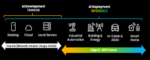
That assumption has a geography. It is Bengaluru — India’s Silicon Valley, where Google, IBM, and Goldman Sachs run core engineering operations indistinguishable from their Western campuses. Hyderabad — Microsoft’s city, home to the largest Microsoft campus outside Redmond. Pune — India’s Wall Street back office, where Deutsche Bank, HSBC, and JPMorgan run the technology backbone of global financial services. And the economy those cities sit inside is more fragile than the corporations building on top of it understand.

India produces roughly 850,000 engineering graduates annually. More importantly it has thirty years of deep integration into Western technology workflows — cloud operations, DevOps, systems architecture, AI/ML engineering. The five largest hyperscalers are collectively worth roughly $13 trillion, more than four times India’s entire GDP. A meaningful portion of the execution capacity those valuations rest on runs through Indian firms. Nobody made a strategic decision to create that concentration. It accumulated through individually rational outsourcing decisions over three decades. That’s exactly the kind of risk that doesn’t appear in models until it becomes obvious.

The direct employment numbers make the concentration concrete. Meta, Apple, Google, Amazon, Microsoft, and Netflix together directly employ around 214,000 people in India — roughly 15% of their combined global workforce, a share that grew 18% in 2025 alone, the fastest rate in three years. The roles filling that growth are not generalist support positions: AI and machine learning operations, data engineering, cloud infrastructure, and cybersecurity — the precise skills the data center buildout depends on — saw demand surge 25–30% year-on-year. That 214,000 is direct employment only. It excludes the Infosys, Tata Consultancy Services, and Wipro engineers running hyperscaler contracts on their behalf. The true India dependency is considerably larger than the direct headcount suggests.

The mechanism has historical precedent

In July 1997, Thailand was a $170 billion economy when its currency peg broke and the baht collapsed. What followed wasn’t contained to Southeast Asia. Indonesia, South Korea, and Malaysia were devastated. Russia defaulted. That default detonated Long-Term Capital Management — a Greenwich hedge fund run by two Nobel laureates and a former Fed vice chair, carrying over a trillion dollars in notional derivatives exposure (real size of the bet, not the money put down to make it) on the premise that global spreads would behave rationally. The New York Fed spent a September weekend in 1998 arm-twisting fourteen banks into a $3.6 billion rescue. The chain ran from a Thai currency pegged at a fixed rate to the dollar to the edge of Wall Street in fourteen months.

The models were excellent. The assumptions weren’t. That combination has a history.

Thailand didn’t cause the 1997 crisis. It revealed it. The vulnerability — dollar-denominated debt accumulated across an entire regional architecture — was already there. The baht collapse was just the match.

India today is twenty times Thailand’s 1997 GDP, with deeper integration into global technology supply chains than any emerging market in history. An India shock wouldn’t create Western AI’s human capital concentration risk. It would reveal it. The kindling is already there.

What the shock looks like

India is not Thailand. It has a floating currency, substantial foreign exchange reserves, and an IMF toolkit available if needed. The trigger would be slower-moving: sustained foreign equity outflows weakening the rupee, raising import costs on an oil-dependent economy, squeezing margins across a corporate sector carrying elevated debt, tightening credit to SMEs (Small and Medium Enterprises), hitting employment. Indian unemployment data is difficult to read — the informal sector dominates, measurement is inconsistent. But Reserve Bank of India (RBI) surveys, CMIE (Centre for Monitoring Indian Economy), which publishes the most reliable independent India labor data, and S&P Global’s India Purchasing Managers Index (PMI) readings would all move in recognizable patterns before the official picture clarified. By then the market signal would already have fired.

The export revenue side of Indian IT is partially insulated — firms billing in dollars while paying costs in rupees can see margin improvement when the rupee weakens. That insulation is shallower than it looks. India’s major IT firms carry substantial domestic revenue exposure to Indian banking, telecom, and government clients. Indian credit markets fund their working capital and expansion. U.S. and European clients watching Indian economic stress on their terminals start asking questions about delivery risk and geographic concentration — some defer contracts, some accelerate vendor diversification — before the dollar revenues move. Foreign revenue is the last thing to go. Everything supporting it goes first.

A sustained shock doesn’t collapse Indian IT. It degrades execution capacity and hiring momentum at exactly the moment global AI infrastructure depends on it most. The data centers get built. The demand they were built to serve arrives late or not at scale. That gap between infrastructure investment and utilization reality is where valuations go to die.

The China asymmetry.

None of this touches China. That is the point.

China’s AI buildout — Huawei’s Ascend ecosystem, Alibaba Cloud, Baidu, ByteDance, DeepSeek — runs on domestic engineering talent inside domestic institutions. Chinese AI does not route through Bengaluru. An India shock is invisible to it.

China graduates nearly 1.5 million engineers annually at the bachelor’s level alone — nearly double India’s output. More importantly, that pipeline points inward. Every U.S. export control restriction on advanced semiconductors accelerated China’s investment in indigenous alternatives. Huawei’s Ascend chips exist because Nvidia’s H100s were restricted. SMIC’s advancing nodes exist because TSMC access was threatened. The export control regime intended to slow China’s AI development instead hardened China’s self-sufficiency.

Washington spent considerable political capital restricting China’s hardware access. DeepSeek answered in January 2024 by producing a frontier model on restricted hardware through algorithmic efficiency. The chip controls didn’t stop China. What they did was redirect China’s talent inward — making China’s entire technology infrastructure — chips, operating systems, cloud platforms, AI frameworks, development tools — more self-sufficient. Meanwhile the West’s own dependency on Indian engineers — the people who actually turn AI infrastructure into working systems inside enterprises — deepened quietly, unexamined, unaddressed, and unnamed in any policy document.

An India shock doesn’t slow both sides equally. China’s AI buildout continues without interruption or friction while the West’s slows down. That is a competitive displacement story, not a slowdown story, and it is playing out inside a technology competition whose participants haven’t fully mapped the battlefield.

The demographic permanence

This is not a temporary market condition that policy can quickly fix.

The United States produces roughly 300,000 computer science and engineering graduates annually. Germany’s federal government has publicly stated that the shortage of skilled workers is severe enough to threaten the country’s economic model. Japan has been in demographic decline for two decades. India and China together produce engineering talent at a scale the rest of the world cannot approach and is not demographically positioned to approach within any relevant planning horizon.

The West built a thirty-year outsourcing dependency on Indian talent without naming it as a dependency. It built a thirty-year manufacturing dependency on China and then spent a decade trying to decouple — export controls, entity lists, visa restrictions — which redirected Chinese talent inward and made China’s technology stack more self-sufficient. The policy apparatus is now tightening H-1B visas and restricting Chinese graduate students in STEM (Science, Technology, Engineering, and Mathematics) programs simultaneously — making the India dependency more acute and the China decoupling more complete, in both cases moving in the wrong direction.

You cannot reshore a demographic curve.

The transmission channels

An India shock moves through four paths.

IT services. India’s IT and Business Process Outsourcing sector generates roughly $200 billion annually. 59% of American companies that outsource IT do so through Indian firms. A hiring freeze at Infosys, Tata Consultancy Services, or Wipro doesn’t stay in Bengaluru — it appears in delayed enterprise implementations, tech sector earnings misses, and hiring signals the Fed watches.

Data center infrastructure. Execution risk introduced into $400 billion in annual hyperscaler investment at the moment Western AI timelines are most exposed and their primary strategic competitor is least exposed. The ribbon cuttings are American. The engineers are not.

Energy. India imports approximately 85% of its crude and roughly 60% of its natural gas through the Strait of Hormuz — the same waterway that has been effectively closed since March 4 by Iranian military action. The Hormuz closure is not a risk scenario for India. It is the current operating environment. Brent crude near $100 a barrel is widening India’s current account deficit toward an estimated 2.9% of GDP. A weakening rupee raises the landed cost of every barrel further, which the government has historically cushioned through subsidies — creating fiscal pressure — or passed through to consumers — destroying demand and feeding inflation. India’s wholesale price inflation surged to 8.3% in April 2026, the highest reading in three and a half years. Over 220,000 Indian nationals have been repatriated from Gulf states as the conflict has displaced the Indian diaspora workforce there, reducing remittances at the same moment the import bill is surging. The energy channel is no longer theoretical. It is the match already lit.

Emerging market contagion. When a large emerging market economy shows stress, institutional investors don’t parse the specifics — they reduce exposure broadly. Currencies from Indonesia to Brazil move. Dollar strength increases. Financial conditions tighten across every dollar-denominated debt market simultaneously. Institutional investors are currently running India exposure through models calibrated on a decade of emerging market stability. Foreign investors pulled $18.4 billion from Indian markets in 2025. The rupee crossed 90 for the first time. The models calibrated on the decade before that aren’t wrong. They’re measuring the world as it usually is, not what it’s becoming.

The bottom line.

Thailand didn’t cause the 1997 crisis. It revealed it. India wouldn’t cause the next one. It would reveal something newer: that the human capital layer of the global AI buildout has a single point of geographic failure, accumulated over thirty years, invisible in the models, and unaddressed in any policy document currently in circulation. The most expensive infrastructure buildout in American technology history is a domestic building wrapped around foreign silicon and foreign human capital. The chips come from an island in the Taiwan Strait. The engineers come from an emerging market no hyperscaler has listed in a risk filing and no presidential directive has named as a strategic dependency. Nobody rang a bell in July 1997 either.

Also Read:

From the Selfie to Samantha: The Next Trillion-Dollar Behavior

Is Intel About to Take Flight?

Who’s Buying America’s Foundry Future?


2026 Outlook with Steve Roddy of Quadric

2026 Outlook with Steve Roddy of Quadric
by Daniel Nenni on 01-27-2026 at 8:00 am

2026 Outlook SemiWiki Image

Tell us a little bit about yourself and your company.

I am the Chief Marketing Officer at Quadric, where I have spent the past four years helping scale the company’s market presence and customer engagement. Quadric is a pure-play IP licensing company that has been operating for more than seven years. We specialize in a truly unique, fully programmable AI inference processor designed for edge and device-level inference, enabling customers to deploy advanced AI workloads without sacrificing flexibility or efficiency.

What was the most exciting high point of 2025 for your company? 

2025 was a breakout growth year for Quadric. Revenue expanded dramatically, reaching the eight-figure range, and multiple customers progressed deep into their tape-out cycles, positioning us to see customer silicon in 2026. We capped off the year by closing a very strong Series C funding round, which further validates both our technology and our long-term market opportunity (announced Jan 14, 2026).

What was the biggest challenge your company faced in 2025? 

The biggest challenge was managing the pace of growth—both in terms of team expansion and customer demand. We roughly doubled our team size and scaled our sales organization to engage with an order of magnitude more prospective customers. It was a classic “good news / bad news” scenario: rapidly growing interest in our technology required more people, more demos, more benchmarks, and more infrastructure; fast.

On the technology side, the most significant shift was the explosive demand for running LLMs and SLMs directly on devices. In 2025, the conversation changed almost overnight from “Is it possible to run an LLM on device?” to “We must run LLMs on device.” On-device LLMs moved from experimental to mainstream far faster than most of the industry anticipated.

How is your company’s work addressing this challenge? 

In 2025, we made major investments in our software infrastructure to enable efficient execution of LLMs on the Chimera processor platform. Unlike traditional CNN- or vision-centric models, modern language models require advanced techniques such as key-value caching (KV cache), which go well beyond simple graph compilation.

Our Chimera Graph Compiler (CGC) ingests AI models, generates optimized C++ representations of those graphs, and targets efficient execution on our processor. However, enabling high-performance LLM inference required additional application-level C++ code beyond graph execution alone. This is where Chimera is fundamentally different from conventional NPU “accelerators.” Chimera runs full C++ applications—not just fragments of an AI model—entirely on the processor.

As a result, we now support a complete software stack for token-based models, including launch, prefill, and KV caching, all running natively on Chimera with no reliance on a companion CPU.

What do you think the biggest growth area for 2026 will be, and why?

The biggest growth area in 2026 will be edge-resident generative AI—particularly LLMs, VLMs, and agent-based models running locally on devices. Market drivers such as latency, power efficiency, data privacy, cost control, and system resilience are pushing intelligence out of the datacenter and onto devices across automotive, industrial, consumer, and infrastructure markets. Customers are no longer willing to compromise between performance and programmability, and that shift strongly favors architectures designed for long-term flexibility.

How is your company’s work addressing this growth? 

Quadric is uniquely positioned to support this growth because Chimera is fully programmable and future-proof by design. As models evolve—and they are evolving rapidly—customers can deploy new networks, operators, and software techniques without changing hardware. Our ability to run complete AI applications in C++, including complex control flow and memory management, enables customers to deploy sophisticated generative AI workloads today and adapt them over time. This dramatically reduces risk for silicon designers planning products with long lifecycles.

What conferences did you attend in 2025 and how was the traffic?

In 2025, Quadric participated in a range of leading AI, semiconductor, and embedded systems conferences. Across the board, traffic and engagement were exceptionally strong. Booth conversations were deeper and more technically informed than in prior years, reflecting a more mature market where customers are actively evaluating deployment strategies rather than simply exploring concepts.

Will you participate in conferences in 2026? Same or more as 2025?

Yes—2026 will be a significant expansion year for us.  We started the year with a big presence at CES in Las Vegas, and throughout the full year we plan to attend more events, increase sponsorships, and focus more on vertical-specific conferences.

How do customers normally engage with your company?

Engagement typically begins with technical briefings and application discussions, followed by hands-on evaluations and benchmarking. Because Chimera™ is highly programmable, customer engagements are often collaborative and long-term.

Additional comments? 

The pace of change in AI is unprecedented, but it is also creating tremendous opportunity for companies willing to rethink traditional hardware and software boundaries. At Quadric, we believe programmability is the key to sustainable AI innovation, and we are excited to help our customers bring advanced intelligence to the edge—without compromise.

Also Read:

Quadric: Revolutionizing Edge AI

Legacy IP Providers Struggle to Solve the NPU Dilemna

Recent AI Advances Underline Need to Futureproof Automotive AI


Hierarchical Device Planning as an Enabler of System Technology Co-Optimization

Hierarchical Device Planning as an Enabler of System Technology Co-Optimization
by Kalar Rajendiran on 01-27-2026 at 6:00 am

Connectivity in a Hierarchical IC Package Floorplan

AI, hyperscale data centers, and data-intensive workloads are driving unprecedented demands for performance, bandwidth, and energy efficiency. As the economic returns of traditional transistor scaling diminish, advanced IC packaging and heterogeneous integration have become the primary levers for system-level scaling. Chiplet-based architectures now dominate this transition, enabling modular design and process optimization but introducing dramatic increases in system and package complexity.

Package pin counts have grown from fewer than 100,000 to tens of millions in leading-edge designs, with further growth expected. This complexity far exceeds what flat design methodologies or manual approaches can manage. System Technology Co-Optimization (STCO) has therefore emerged as a necessary framework for aligning architecture, silicon technology, and packaging. Hierarchical device planning provides the structural foundation required to make STCO effective at scale.

Recently, Siemens EDA published a whitepaper on this very topic and the following is a synthesized overview of that whitepaper. You can download the entire whitepaper from here.

Composable Systems: Reconfiguring 3D ICs for Early System Exploration

Modern systems are increasingly composed of multiple chiplets developed asynchronously and integrated using advanced 3D packaging technologies. While this composability improves flexibility and reuse, it makes early partitioning and integration decisions critical. Hierarchical device planning enables designers to assemble and de-assemble 3D IC systems early in the design process, allowing alternative partitioning, stacking, and interface strategies to be explored before physical commitments are made.

Although detailed layout information is unavailable at this stage, rapid approximate analyses enabled by hierarchical planning provide valuable insight into power integrity, signal integrity, thermal behavior, and mechanical risk. These early insights guide system exploration and prevent costly issues from becoming embedded in the design.

System Technology Co-Optimization (STCO) Begins at Package Planning

Packaging has become a primary determinant of system performance, power, cost, and reliability. Yet silicon design teams often lack early visibility into packaging constraints, leading to partitioning decisions that complicate integration. Hierarchical device planning addresses this gap by enabling fast creation of early package prototypes that support multi-domain analysis.

By generating preliminary bump maps, defining power and signal regions, and placing chiplets in 3D space, designers can evaluate packaging implications early and feed results back to silicon teams. This establishes a continuous, bidirectional feedback loop between architecture, silicon, and packaging, transforming STCO from a sequential handoff into a concurrent optimization process.

Taming Explosive Package Complexity with Hierarchical Planning

The exponential growth in package pin counts has rendered traditional flat planning approaches impractical. Managing millions of pins manually introduces unacceptable risk and inefficiency. Hierarchical device planning overcomes this challenge by decomposing complex package assemblies into structured, hierarchical elements such as chiplets, interfaces, and interconnect regions.

This hierarchical organization enables full-package connectivity tracking and verification across the entire 3D assembly. By providing structure and scalability, hierarchical planning allows designers to manage complexity without losing visibility or control.

Smart Pin Regions and Parametric Abstraction at Scale

A key innovation of hierarchical device planning is the use of parameterized pin regions to abstract connectivity. Instead of defining individual pins, designers work with regions that encapsulate pin patterns, power and ground assignments, and interface characteristics. Pins are automatically synthesized from these parameters, ensuring consistency while dramatically reducing design effort.

CONNECTIVITY IN A HIERARCHICAL IC PACKAGE FLOORPLAN

This parametric abstraction enables rapid iteration. Designers can adjust bump pitch, patterns, or net assignments and instantly regenerate connectivity, supporting fast design-space exploration and efficient response to changing requirements.

A DESIGN OF ARRAYED BLOCKS WITH PARAMETERIZED PINS

Cross-Domain Abstraction and Early Multi-Physics Insight

Effective STCO requires operating at the right abstraction level across electrical, thermal, mechanical, and manufacturing domains. Hierarchical device planning provides this abstraction while enabling early multi-physics analysis. Although early-stage analyses are approximate, they provide sufficient directional guidance to compare alternatives and identify high-risk design choices.

Integrated data management further supports this flow by ensuring consistency across rapidly evolving designs and preventing costly errors caused by outdated or mismatched data.

Summary

As semiconductor systems move toward increasingly heterogeneous and 3D-integrated architectures, managing complexity and cross-domain interaction becomes paramount. Hierarchical device planning enables early system assembly, scalable abstraction, and rapid multi-domain analysis, forming the foundation of effective System Technology Co-Optimization.

By enabling a shift-left design methodology and supporting informed decision-making when flexibility is highest and cost is lowest, hierarchical device planning transforms STCO into a practical, scalable engineering discipline for next-generation electronic systems.

A DESIGN COMPLETED USING HIERARCHICAL DEVICE PLANNING METHODOLOGY

You can download the entire whitepaper from here.

Also Read:

Siemens EDA Illuminates the Complexity of PCB Design

Siemens and NVIDIA Expand Partnership to Build the Industrial AI Operating System

Automotive Digital Twins Out of The Box and Real Time with PAVE360


SiFive to Power Next-Gen RISC-V AI Data Centers with NVIDIA NVLink Fusion

SiFive to Power Next-Gen RISC-V AI Data Centers with NVIDIA NVLink Fusion
by Daniel Nenni on 01-26-2026 at 10:00 am

SiFive Data Center Nvidia NVLink Fusion

In a strategic move that could reshape the future of AI data center design, SiFive, a leading developer of RISC-V processor IP and compute subsystems, has announced plans to integrate NVIDIA’s NVLink Fusion interconnect technology into its high-performance data center platforms. This collaboration bridges the open-architecture innovation of the RISC-V ecosystem with NVIDIA’s industry-leading high-bandwidth interconnects, creating new opportunities for scalable, efficient, and customizable AI infrastructure.

At its core, the partnership is about unlocking seamless, high-speed communication between SiFive’s RISC-V CPUs and NVIDIA’s GPUs and accelerators. NVLink Fusion, NVIDIA’s rack-scale interconnect technology, enables coherent linking of CPUs, GPUs, and other accelerators with extremely high bandwidth. By adopting NVLink Fusion, SiFive’s compute platforms will be able to connect directly to NVIDIA accelerators eliminating the traditional bottlenecks of PCIe-based CPU-to-GPU communication and enabling data center architects to build tightly coupled heterogeneous systems optimized for the demands of AI workloads.

Why This Matters

Artificial intelligence workloads especially large language models (LLMs), recommendation engines, and real-time analytics are rapidly outpacing conventional data center designs. These AI workloads demand not only high throughput, but also efficient data movement and power-optimized compute architectures. Traditional x86- or Arm-based CPUs paired with discrete accelerators over PCIe can struggle to deliver the low latency and high bandwidth required at scale, especially as models grow and power costs skyrocket.

SiFive’s RISC-V IP is prized for its configurability and power efficiency. Customers can tailor processor designs to specific workload requirements, tuning for performance per watt and overall system efficiency advantages that are increasingly valuable in hyperscale environments. Integrating NVLink Fusion expands this value proposition by giving RISC-V CPUs a direct, coherent high-performance path to the acceleration layer of modern AI systems.

NVLink Fusion itself is designed to address the needs of next-generation AI “factories” data centers that treat AI compute as a first-class workload rather than a specialized add-on. The technology offers rack-scale performance and a unified interconnect fabric that scales across hundreds of compute units, significantly improving the performance-per-watt equation for AI training and inference across distributed systems.

Strategic Implications for RISC-V

For years, RISC-V has been touted as the future of open-source compute architecture offering an alternative to proprietary instruction sets like x86 and Arm. However, one of the obstacles RISC-V has faced in the high-performance AI space is ecosystem maturity, especially around high-speed interconnects and software support that large data center players demand.

By aligning with NVIDIA’s NVLink Fusion ecosystem, SiFive helps overcome those barriers. Now, RISC-V processors can participate as “first-class citizens” in rack-scale designs with computed-intensive accelerators, supported by the broader NVIDIA stack including CUDA-based libraries and orchestration tools. This increases RISC-V’s attractiveness for cloud providers, hyperscalers, and custom silicon designers who previously might have defaulted to x86 or Arm platforms due to ecosystem inertia.

In the announcement, SiFive President and CEO Patrick Little emphasized the shift toward co-design in AI infrastructure where open, customizable CPUs are built from the ground up alongside accelerators and interconnects. NVIDIA CEO Jensen Huang echoed this sentiment, framing the partnership as a way to bring coherent, high-bandwidth NVLink into the RISC-V world and enable flexible, scalable AI systems.

Broader Industry Context

This collaboration also signals a broader trend in the semiconductor and data center industries: a move away from one-size-fits-all hardware toward heterogeneous, domain-optimized architectures. Hyperscalers and enterprise data centers alike are investing in bespoke solutions that match compute resources to specific workload profiles, whether that’s training next-generation AI models, delivering low-latency inference, or supporting mixed-use enterprise services.

In addition, NVIDIA’s strategy with NVLink Fusion licensing the interconnect for integration with third-party CPUs expands its ecosystem beyond systems built entirely in-house. By bringing partners like SiFive into the fold, NVIDIA strengthens the adoption of its rack-scale architecture as a de-facto standard for high-performance AI infrastructure.

Bottom Line: The integration of NVIDIA NVLink Fusion into SiFive’s RISC-V data center platforms represents a key milestone for open-architecture AI computing. It combines the flexibility and power efficiency of customizable RISC-V designs with the high-throughput, low-latency fabric needed to unify CPUs and accelerators in modern AI systems. As AI models continue to grow in complexity and scale, such innovations may redefine how data centers are architected — enabling not just faster performance, but smarter, more efficient infrastructure tailored to the real-world needs of AI.

Also Read:

Tiling Support in SiFive’s AI/ML Software Stack for RISC-V Vector-Matrix Extension

RISC-V Extensions for AI: Enhancing Performance in Machine Learning

SiFive Launches Second-Generation Intelligence Family of RISC-V Cores


2026 Outlook with Dave Hwang of Alchip

2026 Outlook with Dave Hwang of Alchip
by Daniel Nenni on 01-26-2026 at 8:00 am

Dave Huang (2)

Dr. Dave Hwang joined Alchip in 2021 as General Manager of Alchip’s North America Business Unit.  He also serves as Senior Vice President, Business Development.  Prior to join Alchip, Dave served as Vice President, Worldwide Sales and Marketing for Global Unichip and in a variety of management and technical roles at TSMC.

Tell us a little bit about your company.

Sure. Alchip is the leading dedicated high-performance ASIC company.  Our company has been publicly traded in Taiwan Stock Exchange since 2014.  Through three quarters of last year, 89% of our revenue was driven by devices designed on 2nm to 7nm technologies.   I’m the General Manager of Alchip’s North America Business Unit, which, through the third quarter of 2025, accounted for 83% of the company’s revenue.

What was the most exciting high point of 2025 for your company?

Oh wow.  I’m not sure you can point to just one thing, because there’s so much going on.  For instance, we taped out multiple customers’ 2nm product test chips based on our groundbreaking 2nm Design Platform.  We also engaged with customers on high performance 2nm full product ASIC development.  We also tapped out multiple 3nm large chip designs with advanced 2.5D packages.  We also formally opened its three-dimensional integrated circuit (3DIC) design services and validated our 3DIC ecosystem readiness with results from its 3DIC test chip tape out.  Last, but not least, we actively began fleshing out our proprietary ASIC system with milestone agreements with a hallmark of technology leaders.

What was the biggest challenge your company faced in 2025?

Our biggest challenge is our high-quality design resource required to fulfill customers’ demand.  Our commitment to customers is to meet their time to market requirements.

How is your company’s work addressing this challenge?

In 2025, part of our engineering focus is to expand our design resource globally. For example, Vietnam and Maylasia.

What do you think the biggest growth area for 2026 will be, and why?

A: Interestingly, I think we’re going to see ASICs replacing standard products in a number of different AI applications.  Industry forecast data shows AI ASIC market growth is accelerating sharply, with estimated revenues expanding from roughly $13B in 2024 to more than $150B by 2030 at a near 50% CAGR, reflecting that hyperscalers are shifting to purpose-built custom silicon. In our opinion, the AI ASICs needed for cloud training and inference will be the highest growth sector among all other segments.

How is your company’s work addressing this growth?

We believe that the winners are going to be those companies who offer excellence across the board.  We continue to invest in the most leading-edge node design implementation and advanced packages from 2.5D to 3.5D.   We work closely with our various ecosystem partners in all aspects to ensure our customer success.

What conferences did you attend in 2025 and how was the traffic?

We attended all of TSMC’s global events, along with Chiplet Summit, AI Infra Summit and the OCP global summit. Traffic at all of the TSMC events was outstanding..

Will you participate in conferences in 2026? Same or more as 2025

Yes, we’ll definitely participate in all TSMC global events and are actively assessing where else we should meet our customers and prospects in 2026.

How do customers normally engage with your company?

That’s always one of my favorite questions, because the answer is that there is no one, single way we engage with our customers.  We engage with our customers at the point that they want to engage.  That’s why we call it “application specific” services.  We’re flexible.  We’re transparent.  We optimize our services to meet each customer’s very specific needs.

Also Read:

Revolutionizing AI Infrastructure: Alchip and Ayar Labs’ Co-Packaged Optics Breakthrough at TSMC OIP 2025

Alchip’s 3DIC Test Chip: A Leap Forward for AI and HPC Innovation

Alchip Launches 2nm Design Platform for HPC and AI ASICs, Eyes TSMC N2 and A16 Roadmap


Agentic at the Edge in Automotive and Industry

Agentic at the Edge in Automotive and Industry
by Bernard Murphy on 01-26-2026 at 6:00 am

Agentic at the edge

It might seem from popular debate around AI and agentic that everything in this field is purely digital, initiated through text or voice prompts, often cloud-based or on-prem. But that view misses so much. AI is already an everyday experience at the edge, for voice-based control, in object detection and safety-triggered braking and steering responses in cars, in predictive maintenance warnings in factories. Now almost so commonplace we may forget that AI underlies those functions. In such use models, demanding real-time response under all conditions, AI must be delivered locally to avoid communication and cloud latencies. Agentic methods are ready to further extend the role of AI at the edge, as I learned in a couple of recent discussions with NXP. For those of who have been curious about “physical AI”, NXP is very much leaning into this area, in software and in hardware.

The value of agentic at the edge

Imagine an industrial shop floor with banks of constantly running engines, monitored by a small number of human supervisors. At some point an engine overheats and bursts into flame. An agentic system detects the incident and takes corrective action: turning on sprinklers while closing (not locking) open doors to limit the spread of fire. Meanwhile it sends a message to the shop-floor manager, providing details of the event. This is an agentic flow. Sensing: perhaps noise, vibrations, certainly video, temperature. Inferencing: detecting and locating the incident. Actuating: turning on sprinklers, shutting doors, turning off power to nearby systems, and sending alerts through text messages.

There are some differences from compute centric agentic systems. Input comes in multiple “modalities” such as motion detection, video, audio, etc. Some are analyzed as time-series and reviewed against prior training. Video and audio analysis similarly are reviewed against pre-training for normal versus anomalous operation. An agentic orchestrator monitors and controls feedback from these agents and can trigger correctives actions as needed.

I talked to Ali Ors (Global Director of AI Strategy and Technologies for Edge Processing at NXP) on their recent announcement of a cloud-based eIQ AI hub and toolkit. This platform supports developing and accelerating agentic AI at the edge for applications like this factory example, or for other areas (automotive, avionics and robotic). eIQ AI targets a range of NXP hardware platforms offering AI support, from MCUs up to S32N7 processors (see the next section) and discrete NPUs including their Ara platform.

eIQ AI builds on established industry standards and emerging standards for agentic systems to provide a lot of functionality right out of the box. Leveraging these capabilities, NXP have been working with ModelCat who provide support to build custom agentic models in days rather than years. This is incredibly valuable because few companies today have armies of PhD data scientists to build and maintain agentic models from scratch. For problems they need to solve today, not years from now.

There’s another point I consider very important. In general discussion around mainstream digital agents and agentic systems, high accuracy and security still seem to come across in practice as a goal rather than a near-term requirement. That is not good enough for these physical AI applications. While NXP do not themselves build deployed agentic solutions, they provide significant infrastructure (safety, security, multiple AI and non-AI engines able to run in parallel) to support their customers and customers’ customers to meet these much more demanding targets.

NXP S32N7 promotes agentic innovation

The old approach to electronic control in a car, distributing MCUs around engine, body and cabin control functions, is now impractical. Architectures have evolved to more centralized hierarchies, consolidating more capabilities and control in zonal functions. Nicola Concer (Senior Product Manager, Vehicle Control and Networking Solutions, NXP) shared insight into ongoing motivation for consolidation. NXP has a widely established and dominant gateway (automotive networking) product called S32G. Already this gateway touches almost everything within a network connected car. Given this reality, customers have asked NXP to take the next logical step. Could they integrate into that same platform: motion intelligence, body intelligence, ADAS intelligence? Consolidating that hardware and software in the S32N7 increases performance and reduces cost while simplifying design and maintenance.

Which for me prompted a question: will these devices serve as zonal controllers or as zonal and central controllers? Nicola told me I shouldn’t think of an architecture in which everything coalesces into one giant central controller or a central controller with one level of branching to zonal controllers. Think of a more general tree in which some branches may themselves sprout branches. An OEM architects a hierarchy to meet fleet objectives while also standardizing on a family of common controllers. The root device may be something else, say for autonomous driving, but NXP can manage the rest of the tree, offering ample opportunities for innovation.

The standard way for OEMs/Tier1s to innovate is be simply to enhance existing features. But Nicola suggests bigger opportunities to stand out are through inferences across domains. Here’s a simple example: You park, want to open your door, but a car is approaching from behind. Cross-domain inference detects the car through radar, detects you are trying to open your door and sounds an alarm, maybe even resists you opening the door.

There are many other such opportunities, when driving, when stationary, when charging your car, and so on. Sensing, inferencing and actuating in each case. All powered by agentic methods.

The S32N7 together with eIQ enables this innovation. Agentic here can run agents on application or real-time cores. They can run models on embedded NPUs within the processor, maybe to infer tire status through tire pressure time series. Or to infer tire noise for active noise cancellation inside the cabin. For more complex inferences, an orchestrator can communicate through PCIe to a discrete Kinara NPU plugged in as an AI expansion card. Multiple paths to an inference also allow for cross checking by comparing answers generated through different paths, an important safety consideration in some cases.

Very impressive. For me this is an inspiration showing that high fidelity, high safety agentic options are a real possibility. Maybe some of these ideas can flow back into cloud-based agents? You can read more about the eIQ platform HERE and the S32N7 family HERE.

Also Read:

2026 Outlook with Kamal Khan of Perforce

Curbing Soaring Power Demand Through Foundation IP

Automotive Digital Twins Out of The Box and Real Time with PAVE360


TSMC’s CoWoS® Sustainability Drive: Turning Waste into Wealth

TSMC’s CoWoS® Sustainability Drive: Turning Waste into Wealth
by Daniel Nenni on 01-25-2026 at 12:00 pm

TSMC's CoWoS® Sustainability

In a significant example of how high-tech manufacturing can embrace environmental stewardship without compromising operational excellence, Taiwan Semiconductor Manufacturing Company has launched a sustainability initiative within its advanced packaging operations that both reduces waste and generates meaningful economic value. This drive, centered on TSMC’s CoWoS® (Chip on Wafer on Substrate) advanced packaging technology, demonstrates how innovation in recycling and circular practices can transform manufacturing byproducts into valuable resources resulting in annual green benefits of approximately NT$700+ million ($22M+ USD), alongside substantial carbon reduction.

At the heart of this sustainability effort is the repurposing of scrap or “waste” wafers, silicon discs produced and later deemed unsuitable during front-end production. Traditionally, such wafers are discarded once they fail to meet performance or quality specs. However, these silicon substrates still contain high-grade material and structural integrity valuable for secondary uses. Recognizing this, TSMC’s Materials Supply Chain Management Organization, in collaboration with its Advanced Packaging Technical Board and external suppliers, developed a specialized processing technology that turns scrap wafers into dummy dies, components essential in the CoWoS packaging process to maintain structural stability.

Dummy Dies and CoWoS®

To understand the significance of this initiative, one must appreciate the role of dummy dies in advanced semiconductor packaging. In CoWoS® technology, multiple active chips are stacked and integrated onto an interposer and substrate to create powerful multi-chip modules for high-performance computing, AI accelerators, and networking devices. During this process, dummy dies are inserted to fill space, balance mechanical stress, and maintain uniform thermal and electrical profiles. These are typically cut from brand-new wafers, which makes them a non-trivial fraction of packaging consumption—especially as demand for CoWoS® scales with burgeoning markets like AI, cloud computing, and advanced graphics.

Instead of using all new wafers to produce these dummy dies, TSMC’s cross-functional team developed a rigorous recycling methodology for scrap wafers. This involves selection, grinding, cleaning, and precision inspection to ensure recycled wafers meet the same strict quality requirements as newly sourced material. After processing, these recycled wafers are cut into dummy dies that are functionally and structurally suitable for CoWoS® assembly. This innovation not only salvages silicon that would otherwise go to waste, but also significantly shifts material sourcing dynamics toward sustainability.

Economic, Environmental, and Operational Impact

Early reports on the initiative’s outcomes have been compelling. As of late 2025, recycled wafers re-manufactured into dummy dies have been deployed across multiple advanced backend facilities, including Advanced Backend Fab 3, Fab 5, and Fab 6. The result is an estimated reduction of 10,205 metric tons of carbon emissions annually, underscoring a meaningful contribution toward TSMC’s broader climate goals. On the financial front, TSMC anticipates that this reuse of scrap wafers will generate a green benefit amounting to NT$746 million per year surpassing the NT$700 million mark cited in sustainability narratives.

This initiative exemplifies a practical circular economy model within semiconductor manufacturing: instead of viewing scrap material as waste to be disposed of at environmental cost, it becomes a resource to be refined and reintegrated into production. Beyond direct savings and emissions reductions, there are supply-chain ripple effects that encourage vendors and partners to invest in recycling technologies, improve material lifecycle tracking, and innovate in waste valorization.

TSMC’s approach aligns with its broader Environmental, Social, and Governance (ESG) strategy, which emphasizes resource circularity, energy efficiency, and environmental protection across its global operations. The company has consistently integrated sustainable practices—such as waste recycling programs and comprehensive environmental management—into its long-term operational blueprint.

Looking Forward

Looking ahead, TSMC plans to further expand the scope of recycled wafer use across different packaging technologies and processes, potentially including InFO (Integrated Fan-Out) packaging and beyond. By continually optimizing these techniques and extending collaboration across its supply chain, the company seeks to maximize resource efficiency while maintaining the highest product quality standards, a hallmark of its global leadership in semiconductor manufacturing.

Bottom line: TSMC’s CoWoS® sustainability drive encapsulates how bold environmental action and industrial innovation can work hand-in-hand, turning what was once waste into wealth economically and ecologically alike.

Also Read:

TSMC’s 6th ESG AWARD Receives over 5,800 Proposals, Igniting Sustainability Passion

TSMC based 3D Chips: Socionext Achieves Two Successful Tape-Outs in Just Seven Months!

Why TSMC is Known as the Trusted Foundry


Podcast EP328:A Brief History of Chip Design and AI with Dr. Bernard Murphy

Podcast EP328:A Brief History of Chip Design and AI with Dr. Bernard Murphy
by Daniel Nenni on 01-23-2026 at 10:00 am

Daniel is joined by Dr. Bernard Murphy, a friend and fellow blogger on SemiWiki.

Dan explores some key milestones in Bernard’s journey in semiconductors and EDA, beginning with a focus on nuclear physics. Bernard explains how he developed an interest in AI technology and applications. In this broad and informative discussion, areas where AI is in use today for chip design are explored. Bernard also comments on where AI will find application in the future. Dan and Bernard discuss the question of whether AI will replace design engineers. Bernard also discusses his role as a contributor to Forbes and how that fits into his overall plans.

The views, thoughts, and opinions expressed in these podcasts belong solely to the speaker, and not to the speaker’s employer, organization, committee or any other group or individual.