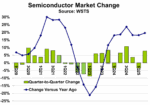
SNPS1670747138 DAC 2025 800x100px HRes

ML and Multiphysics Corral 3D and HBM

ML and Multiphysics Corral 3D and HBM
by Bernard Murphy on 01-07-2025 at 6:00 am

multidie and HBM stacks min

3D design with high-bandwidth memory stacks (HBM) has become essential for leading edge semiconductor systems in multiple applications. Hyperscalers depend on large AI accelerator cores supported by 100GB or more of in-package HBM to handle trillion parameter AI models. Autonomous Drive (AD) vehicles may handle smaller individual tasks but more of them through multiple levels of sensing and fusion support, computer vision, graphics, safety, security, and communication objectives. Similar requirements are appearing in aerospace and other applications. All require 3D integration with HBM to maximize performance, minimize latency, and minimize power consumption. Manufacturing technologies to build such systems are already in place but optimizing such a design introduces new physics challenges in performance and reliability.

The Physics of Large System Design

There’s only so much circuitry you can fit on a single silicon die, even in the most advanced processes. Bigger designs must split across multiple chiplets (die) but can now connect very effectively inside a single package, greatly reducing the performance and power hit compared to an equivalent circuit between packaged components on a PCB. The advantage is especially clear for large memory access implemented as stacked HBM chiplets within the same package, for which access latencies are greatly improved over off-chip DRAM.

Managing the physics of large semiconductor designs was already prominent before multi-chiplet designs appeared. Beyond the usual design objectives (functionality, performance, power and area/cost) a product design team must optimize for: over-heating with potential to damage/compromise the system; inadequate power distribution for functional demand undermining performance and reliability; electronic crosstalk impacting signal integrity; die/chiplet warping through heating resulting in broken bond connections. Tools to analyze these factors for a single die are already familiar and a well-understood strength for Ansys: power integrity (EM/IR) analysis, thermal analysis, signal integrity and mechanical analysis coupled with thermal.

Scaling multiphysics analysis up to multi-chiplet designs introduces new challenges. Thermal becomes a bigger issue especially in stacked structures where thin chiplet substrates provide little thermal isolation between layers. This analysis problem isn’t just bigger than for an already complex single die multiphysics analysis; in a 3D/HBM structure all these factors are coupled and must be co-optimized.

Multiphysics, Coupling and ML

Lang Lin (Principal Product Manager at Ansys) gave an excellent webinar talk recently on this topic, illustrating with emphasis on an HBM stack, sitting on top of a logic die and next to CPUs or GPUs on the interposer. One point he made is that traditional PVT (process-voltage-temperature) corner analysis for a single die won’t necessarily work for analysis of a complete structure of stacked chiplets. In an HBM stack, chiplets may have different assembly corners due to coupling effects. One might best be assigned a temperature of 90 degrees, at 0.8 volts and a fast-fast process. Another (in the same stack) should be assigned a temperature of 100 degrees, 0.9 volts and a typical-typical process. And so on, down the stack. Raising an obvious question – how do you figure this out?

A key point Lang made is that physics factors in this tightly packed environment are strongly coupled and all centered around thermal considerations.

Coupling implies that you can’t just optimize for one factor at a time. Temperature affects the power delivery network, timing, signal integrity which in turn can affect temperature. In a heterogenous integration with HBM, CPUs, GPUs, etc., etc., optimizing across all these factors would become a nightmare. Converging to an optimal physics solution requires (no surprise) intelligent and automated guidance. Ansys accomplishes this through their OptiSLang system which will search intelligently through vast parametric spaces to find robust solutions automatically. I’m convinced this is the way of the future in system level optimization tasks of all kinds.

Ground Proofs

Lang illustrated with a couple of live examples, the first working with TSMC on HBM optimization for warpage/stress in assembling a stack, which can result in yield loss. Here thermal cycling is based on manufacturing requirements rather than on use-cases, however I would think that temperature ranges they show in manufacturing are at least as stressful as in mission mode. TSMC and Ansys used the flow to estimate warpage/stress at each assembly step, to come up with an optimal manufacturing assembly sequence.

In another case study, Ansys worked with a different company to optimize the signal integrity of high-speed HBM interconnect (connecting to compute chiplets) on a 2.5D interposer. Here they were able to propose an optimal routing pattern for the multi-bit interconnect to minimize (transmission line) overshoot.

Pretty impressive. You can register to watch the webinar HERE.

Also Read:

A Master Class with Ansys and Synopsys, The Latest Advances in Multi-Die Design

Synopsys-Ansys 2.5D/3D Multi-Die Design Update: Learning from the Early Adopters

Ansys and eShard Sign Agreement to Deliver Comprehensive Hardware Security Solution for Semiconductor Products


CES 2025 and all things Cycling

CES 2025 and all things Cycling
by Daniel Payne on 01-06-2025 at 10:00 am

UrbanGlide 3

CES 2025 was held from January 7-10, once again in Las Vegas, so I attended virtually to gather together all of the tech and trends related to cycling, which is becoming more electrified each year. E-bikes return as the biggest category and from my cycling rides I can see how popular these bikes are becoming in Oregon for commuters and people that enjoy being outdoors more without having to sweat as much. The latest e-bikes have electric motors and batteries neatly hidden and integrated into the frame or rear hub, along with a display on the handlebars to let you know how much charge remains and other metrics.

E-Bikes

This is still the fastest-growing and most profitable sector in the cycling world, with higher ASPs than pedal-powered bikes

Livall conversion kit

With this accessory your regular bike can be converted into an e- bike, as it connects to the seat tube and moves your rear wheel by friction. It even earned a 2025 Innovation Award from CES. I question the efficiency of power transfer and the robustness of the design, but marvel at the retrofit market.

LIVALL PikaBoost 2

Urtopia – Titanium e-bike

This e-bike has a strong frame made from titanium, great for commuting or gravel riding and compatible with traditional shifting, weighing only 23.8 pounds.

Urtopia Titanium Zero

Urtopia

Yes, with some AI technology called ChatGPT this bike provides navigation, safety alerts and gives motivation to stay fit. Comes in three models.

Fusion GT

Vanpowers

Four e-bike models were shown this year at CES, and the UrbanCross-Ultra provides a 60 nile range.

UrbanCross-Ultra

For off-road cycling there’s the GrandTeton-Ultra with a 65 mile range.

GrandTeton-Ultra

If you prefer a fat tire e-bike, then there’s the Cycanon with a 60 mile range.

Cycanon

Urban commuting with shocks and a rack are found in the UrbanGlide-Standard e-bike.

UrbanGlide-Standard

Muon

This German-based vendor has e-bikes in several styles, all named after elementary particles: Elon, Axion, Lepton, Bradyon. Some of their models use a belt drive, instead of a chain for easier maintenance.

Elon

ENGWE

This brand has multiple e-bike categories: commuter, fat-tire off road, folding, step-through, e-scooter. The M20 2.0 looks more like a motorcycle, has an 80 mile range, and comes with complete suspension.

M20 2.0

Blaupunkt

I remember this brand mostly for their car audio gear, and they’ve expanded into Class 2 e-bikes which have a 40 mile range, while being foldable.

Fiene eBike

SOL

A 2025 CES Innovation Award honoree, SOL showed off their Pocket Rocket S, capable of 55 mph speeds and a 70 mile range. The design is rather artistic, looking like you’re sitting on a cylinder rocket.

Pocket Rocket S

HIMIWAY

This Shanghai-based company offers a full-range of e-bikes:  mountain, kids, city, cargo, folding, step through, full suspension, motorbike.

City eBike

Heybike

They showed several new models of e-bikes this year: Polaris, Helio, Alpha (commuter), X (folding).

Helio Series

AIMA

With 400 dealers around the globe, this brand offers  e-bikes with a 20-inch fat tires – Big Sur, and a step-thru bike with 750W motor – Santa Monica.

Santa Monica

OKAI

Another company from China with a presence in Europe and North America is showing off a line of five e-bikes and eight e-scooters this year.

OKAI

Bosch

From Germany we have e-bike motors and apps.

Bosch Technology

C-Star Industrial Limited

From Shenzhen, China this 24 year old company showed off their e-scooters.

CS-P14

Komda

Based in Hong Kong, this vendor has a range of e-bikes: cargo, mountain bike, folding, city. They also offer traditional bikes: kids, folding, city.

Electric Cargo Bike

Moqous

From South Korea comes a new company that provides both a folding e-bike, and pedal bike designed for people that want to conserve space and have short commutes.

Pop-Cycle-E

Oh Wow

Offering both e-bikes and e-trikes, this California company has many models to choose from.

Conductor Trike


Altovetti

It sounds Italian, but this is a Chinese brand with a step-through e-bike, available in a variety of colors, designed for commuting.

Altovetti

Rundeer

Designed for off-road and commute use, this company offers three models.

Rundeer Starry Sky

Spard

All of these e-bikes require a battery and that’s where Spard comes in, supplying the many different battery form factors: external, in-tube, dual system, bottle cage, integrated, semi-integrated, rear carrier.

e-bike battery

Pedal Bicycles

Biky

This brand has kids bikes that look like a lot of fun to get started in cycling.

Biky Air 12

Trainers

On rainy or cold days a cyclist can opt to ride indoors using some type of trainer setup.

Speediance

At first this looked just like another Peleton competitor, but it actually integrates with all the popular platforms: Zwift, Strava, Apple Health, Samsung, Garmin.

VeloNix

Yesoul

A spin bike with integrated display in a few models from this Chinese vendor where you follow sessions to stay fit.

Yesoul G1M Max

Garmin

This American brand has a range of indoor trainers from low-cost on-wheel, up to their smart trainers that work with popular apps like Zwift.

Tacx Flux 2

VirtuRide

This spin bike comes with a VR headset, so you get to view real terrain while your bike tilts side-to-side, and even heads up and down hill.

VirtuRide

Real Design Tech

Smart rollers with a sturdy arm to hold your bike upright, keeping you from falling over, and compatible with the most popular indoor cycling app Zwift.

Ultiracer

Sunny

Offering over 20 varieties of trainers, you will find something to fit your taste and budget.

Smart Pro Belt Drive Indoor Cycling Exercise Bike

Accessories

Alps Alpine

This rear-facing camera sends a live view to a display on your handlebars of traffic coming from behind you, keeping you safer from motorists.

RS 1000 Bike Camera


Aizip

Trek Bike and Aizip collaborated to create a demo of a Small Language Model Assistant for biking, bringing together Aizip technology and Trek Bike domain expertise. The Trek e-MTB has an Aizip demo helmet to make off-road rides and routes easier to plan, so that you don’t get lost,  recommend new routes, offer coaching and provide a safety alert in case of a crash.

Aizip and Trek

Livall

Smart helmets for road and mountain bikers include lighting to indicate braking, fall detection and SOS alert, voice navigation, and an alarm for security. My friends with rear lights on their helmets really improve visibility for motorists, as the high position of the lights are closer to eye level.

BH60SE Neo

SuperTooth

This gizmo clips onto your existing bike helmet and provides a hands-free Bluetooth connection for listening to music, making phone calls, or as an intercom, all while cancelling out wind noise.

Roamee

aabo

Instead of measuring heart rate on a chest-strap monitor, why not use a ring that also tracks your sleep, stress and other physical activities?

aaboRing

CRNK

Protecting your head while cycling is paramount to safety and CRNK has designed over a dozen models, and some have added lighting to improve visibility.

Genetic Alpha

Circular

Another ring-based fitness device to monitor your heart rate along with haptic feedback and an app to show you what’s happening throughout the day and even sleep time.

Circular Pro

Garmin

A long-time provider of bike computers ranging from entry-level to the flagship 1050 device.

Garmin 1050

Riduck

Get some pro-level cardio training with this AI-based app that looks at your heart rate monitor and cycling power meter data recorded by Strava. Learn what your FTP, VO2MAX and FATMAX numbers are.

Riduck app

Bosch

Locking your e-bike makes sense, but adding even more security comes from Bosch’s eBike Lock system that turns your battery off when you step away from the e-bike. A thief can still cut your physical bike lock off, but then be stopped from riding your e-bike away with any motor support as the battery is still turned off. You install an app on your phone, or use the Bosch Kios or Nyon e-bike removable displays as your key to unlock or lock the battery.

eBike Lock


Related Blogs


Can LELE Multipatterning Help Against EUV Stochastics?

Can LELE Multipatterning Help Against EUV Stochastics?
by Fred Chen on 01-06-2025 at 6:00 am

Can LELE Multipatterning Help Against EUV Stochastics

Previously, I had indicated how detrimental stochastic effects at pitches below 50 nm should lead to reconsidering the practical resolution limit for EUV lithography [1]. This is no exaggeration, as stochastic effects have been observed for 24 nm half-pitch several years ago [2,3]. This then leads to the question of whether using multipatterning to get below the practical resolution limit can be of any help in avoiding these stochastic effects.

Multi-patterning in its most basic form involves forming a layer pattern with at least two mask exposures. In the simplest case, the LELE (Litho-Etch-Litho-Etch) approach, the target layer pattern is divided into two portions, which are combined by interleaving features such as lines. This is necessary when a single exposure cannot resolve (without defects, deformation, or feature loss) the minimum pitch between two features. The two features separated by this minimum pitch must then be exposed separately. For example, two 15 nm lines separated by 30 nm pitch would need to have two exposures: a first exposure to pattern one 15 nm line in resist, followed by an etch, and a second exposure to pattern the second 15 nm line in a subsequently recoated resist, followed by the etch.

Given that 15 nm lines on 30 nm pitch are known to be impacted by stochastic effects, it is natural to ask whether the same lines fare better on 60 nm pitch. Figure 1 shows a qualitative comparison. Without the actual mask structure details being known, a classical binary grating is used to represent the mask, and the illumination is the dipole used for 30 nm pitch, which will generated two beams from the mask for the 30 nm pitch case, and three beams from the mask (1st order being the middle beam) for the 60 nm pitch case. The same simulation model and conditions were used as in [1].

Figure 1. A 15 nm drawn line on 60 nm pitch (left) and 30 nm pitch (right). The same illumination is used for both cases (dipole for 30 nm pitch). The lines were modeled using binary grating features as the mask pattern. Under the shown modeling conditions, the 60 nm pitch is slightly better due to the higher photon and electron density in the exposed area.

The photon density happens to be higher for the 15 nm drawn line on 60 nm pitch. However, the NILS of the 15 nm line on 60 nm pitch is lower than on 30 nm pitch (1.7 vs. 2.8 even without blur). This means more pixels within the exposed region have a higher chance of the local photon density dropping below the threshold to become defective. The dark defect pixel % is a little lower for the 60 nm pitch compared to 30 nm pitch (~23% compared to ~30%). While it visually looks a little better, the edge definition from the scattered electron density is still poor. In addition, the stochastic defect rate has been found to be higher when the CD is less than the half-pitch [5,6]. Therefore, we must conclude that LELE patterning does not help avoid detrimental stochastic effects. The key reason is the CD being printed is still too small.

A way around this is to use spacers to define the CD. This is used in self-aligned double patterning (SADP) as well as SALELE (self-aligned LELE) [6]. This allows larger features to be printed by the exposure, e.g., 30 nm instead of 15 nm on 60 nm pitch. Interestingly, at around 40 nm pitch, double patterning by SADP or SALELE may overlap for DUV and EUV, since stochastic effects still look severe at 40 nm pitch [1], while 80 nm pitch is achievable by DUV single exposure [7].

Thanks for reading Exposing EUV! Subscribe for free to receive new posts and support my work. Pledge your support here.

References

[1] F. Chen, Stochastic Effects Blur the Resolution Limit of EUV Lithography.

[2] D. van den Heuvel et al., “Process Windown Discovery Methodology Development for Advanced Lithography,” ASMC 2016.

[3] S. Das et al, “E-beam inspection of single exposure EUV direct print of M2 layer of N10 node test vehicle,” Proc. SPIE 10959, 109590H (2019).

[4] P. de Bisschop and E. Hendrickx, “On the dependencies of the stochastic patterrning- failure cliffs in EUVL lithography,” Proc. SPIE 11323, 113230J (2020).

[5] J. Church et al., “Fundamental characterization of stochastic variation for improved single-expose extreme ultraviolet patterning at aggressive pitch,” J. Micro/Nanolith. MEMS MOEMS 19, 034001 (2020).

[6] F. Chen, SALELE Double Patterning for 7nm and 5nm Nodes.

[7] H. Hu et al., “K=0.266 immersion lithography patterning and its challenge for NAND FLASH,” CSTIC 2015.

Also Read:

Stochastic Pupil Fill in EUV Lithography

Application-Specific Lithography: Patterning 5nm 5.5-Track Metal by DUV

Why NA is Not Relevant to Resolution in EUV Lithography


WEBINAR: 2025 Semiconductor Year in Preview

WEBINAR: 2025 Semiconductor Year in Preview
by Daniel Nenni on 01-03-2025 at 6:00 am

Webinar 2025 semiconductor year in preview

TechInsights has been in the semiconductor analysis business for more than 35 years and is THE most trusted source of semiconductor information. TechInsights started as a reverse engineering and IP analysis company but has grown into much more. I remember waiting for the teardown reports before buying electronics to make sure I knew what was inside. Now I read them to get detailed information on semiconductor process technologies.

SemiWiki blogger Scotten Jones sold his company IC Knowledge to TechInsights two years ago and before that TechInsights bought Dan Huctheson’s research company VLSI Design. They also acquired The Linley Group and The McClean Report amongst others. Rest assured, our semiconductor secrets are safe with TechInsights.

To start the new year TechInsights is hosting a free webinar preview of 2025. I hope to see you there:

2025 will be an eventful year in the semiconductor industry—don’t expect the unexpected, be prepared!

Join TechInsights experts behind The McClean Report for our latest webinar 2025 semiconductor year in preview. Get advance insight into the key events in 2025 and what they mean to your business:

Register: January 15, 2025 – 10:00 AM EST
Register: January 16, 2025 – 11:00 AM JST / KST

Key Topics to be Covered:
2025 Tariff Shake-Up: Are You Ready?

January starts with a new US administration promising to shake up tariffs—what are the scenarios you should plan for?

NVIDIA vs. AMD & Intel: AI Accelerator Showdown

In March, NVIDIA will unveil the successor to GraceHopper, and later in the year AMD and Intel will launch next generation AI accelerators. Will NVIDIA keep its crown?

2nm Breakthroughs: Intel, TSMC, and Rapidus Lead

2025 will be the year of 2nm and beyond, with Intel 18A and TSMC N2 coming online in the first and second half of 2025 respectively, and details of Rapidus’ 2nm process expected to emerge.

And that’s not all… Altera, Cerebras, Coreweave, KIOXIA, and SanDisk will all woo Wall Street with new listings, Apple will launch new devices at WWDC in June, and HBM4 specifications will be announced. 2025 will be an eventful year in the industry—don’t expect the unexpected, be prepared!

Presenters:

David MacQueen, Director, Executive Insights and James Sanders, Senior Analyst.

As the Director, Executive Insights, David MacQueen is tasked with covering the semiconductor value-chain to identify emerging technologies and new opportunities for research teams, while ensuring alignment across the research produced by TechInsights. He has over 20 years of experience in semiconductor-related industries and has an inherent ability to contextualize data that helps clients understand the big picture.

James Sanders is a Senior Analyst at TechInsights with over 5 years of experience as an industry analyst, and 7 years of experience as a technology journalist. James has a passion for researching the innovations being made possible through high performance and quantum computing and is fascinated by application processor and system architecture design that enables these innovations. He enjoys having the ability to work closely with clients and provide insights on the value and utility of these new advancements.

About TechInsights

Regarded as the most trusted source of actionable, in-depth intelligence related to semiconductor innovation and surrounding markets, TechInsights’ content informs decision makers and professionals whose success depends on accurate knowledge of the semiconductor industry—past, present, or future.

Over 650 companies and 100,000 users access the TechInsights Platform, the world’s largest vertically integrated collection of unmatched reverse engineering, teardown, and market analysis in the semiconductor industry. This collection includes detailed circuit analysis, imagery, semiconductor process flows, device teardowns, illustrations, costing and pricing information, forecasts, market analysis, and expert commentary. TechInsights’ customers include the most successful technology companies who rely on TechInsights’ analysis to make informed business, design, and product decisions faster and with greater confidence. For more information, visit www.techinsights.com.

Also Read:

5 Expectations for the Memory Markets in 2025

VLSI Technology Symposium – Intel describes i3 process, how does it measure up?

Intel High NA Adoption


Accelerating Automotive SoC Design with Chiplets

Accelerating Automotive SoC Design with Chiplets
by Kalar Rajendiran on 01-02-2025 at 10:00 am

System Chiplet

The automotive industry is evolving rapidly with the increasing demand for intelligent, connected, and autonomous vehicles. Central to this transformation are System-on-Chip (SoC) designs, which integrate multiple processing units into a single chip for managing everything from safety systems to in-car entertainment. However, as these systems become more complex, traditional SoC designs face challenges around performance, power, and scalability. Chiplet-based architectures are now driving innovation by offering more flexible, efficient, and customizable solutions for automotive SoCs.

Cadence recently hosted a webinar on this topic, with Moshiko Emmer, a Distinguished Engineer for the company’s Silicon Solutions Group (SSG) presenting.

Benefits of Leveraging Chiplets in Automotive SoC Design

Chiplet-based designs are reshaping automotive SoC development by offering a modular and scalable approach. Each chiplet, such as CPU cores, memory units, or specialized processing units like NPUs, is a self-contained module that can be easily integrated into larger systems. As automotive systems advance, especially with ADAS, infotainment, and autonomous driving, chiplet architectures provide several key advantages.

-Enable engineers to focus on specific value-added functions, reducing development time, cost, and risk while improving time-to-market.

-Allow for highly scalable designs, meeting the varying performance and power needs of different vehicle segments.

-Ensure long-term cost efficiency and adaptability to new technologies through reuse of chiplets across multiple generations of SoCs

By combining off-the-shelf chiplets with specialized automotive IP, manufacturers can build comprehensive solutions, benefiting from a broad ecosystem of reference designs and industry-standard IP.

Accelerating Automotive SoC Design

Adopting chiplet-based designs for automotive SoCs involves several essential efforts to ensure performance, safety, and reliability.

Chiplet Frameworks

A robust chiplet framework ensures the seamless integration of chiplets from different vendors. Standardized protocols and interfaces, such as UCle™, streamline the integration process, allowing for more efficient chiplet-based SoC designs. Cadence’s System Chiplet framework enables designers to integrate and connect multiple chiplets in a cohesive architecture, facilitating high-performance, scalable designs tailored for automotive applications.

SoC Design Cockpit

The SoC Design Cockpit approach helps automate the design process with correct-by-construction tools, ensuring that the final system meets all performance and safety requirements. This platform enables extensibility for customizing automotive-specific features like real-time processing and high-speed data handling. For example, the Cadence System Chiplet comes with pre-designed frameworks for automotive applications, allowing engineers to quickly select the necessary chiplets and integrate them efficiently into a full SoC. The cockpit’s automated tools help reduce manual intervention, ensuring high-quality and safe designs for automotive use.

Virtual Platforms

Virtual platforms enable early software development before hardware is available, which is especially valuable for complex systems like ADAS and infotainment. Tools like Cadence Helium™ software digital-twin allow engineers to simulate hardware, test software, and avoid costly errors before physical hardware is built. By integrating Cadence’s Neo NPU chiplet, which is designed for AI and machine learning tasks, into a virtual platform, developers can simulate the performance of advanced automotive applications such as real-time object detection, predictive analytics, and autonomous driving algorithms.

Design Services and Ecosystem Collaboration

Collaborating with design services partners and leveraging off-the-shelf chiplets accelerates the integration of complex systems such as sensor fusion and machine learning. Working within a broad ecosystem of partners can also speed up the development of automotive SoCs. Cadence’s Neo NPU chiplet enables integration with machine learning workflows, supporting the development of intelligent, real-time systems for automotive applications. Together with the System Chiplet framework, these chiplets facilitate rapid prototyping and customization, accelerating time-to-market.

Chiplet Testchips: Ensuring Automotive SoC Reliability

Given the critical nature of automotive applications, ensuring the reliability and safety of chiplet-based SoCs is paramount. Chiplet testchips validate the performance and functionality of individual chiplets before integration into the full SoC. Testchips are essential for verifying that chiplets meet the functional requirements of automotive systems like ADAS and infotainment, as well as for ensuring compliance with safety standards such as ISO 26262.

Summary

Chiplet-based architectures are transforming automotive SoC design by offering scalable, customizable, and cost-efficient solutions. By leveraging Cadence’s System Chiplet and Neo NPU chiplet frameworks, as well as tools like the SoC Design Cockpit and Cadence Helium™ software digital-twin, automotive manufacturers can accelerate the development of next-generation vehicle technologies like ADAS, autonomous driving, and infotainment. Chiplet testchips further ensure the reliability and safety of these designs. As chiplet technology continues to evolve, it will unlock new opportunities for the automotive sector, driving smarter, safer, and more connected vehicles.

For more details, refer to the following:

Cadence Automotive Solutions page.

You can access this webinar on-demand from here.

Also Read:

Accelerating Simulation. Innovation in Verification

Accelerating Electric Vehicle Development – Through Integrated Design Flow for Power Modules

Compiler Tuning for Simulator Speedup. Innovation in Verification


AI PC momentum building with business adoption anticipated

AI PC momentum building with business adoption anticipated
by Don Dingee on 01-02-2025 at 6:00 am

Growth in AI hardware IP leads to AI PC momentum

And just like that, the AI PC arrived. It will be hard to miss high-profile advertising campaigns like the one just launched by Microsoft touting them. Gartner said this September that AI PCs will be 43% of all PC shipments in 2025 (with 114M units projected) and that by 2026, AI PCs will be the only choice for business laptop users. Other analysts are going with even bigger numbers. The idea of an AI-enabled personal assistant is intriguing, and with AI PC momentum building fast, waiting to create and adopt implementations may be an expensive miss. We spoke with Ceva’s Roni Sadeh, VP of Technologies in their CTO office, to get some insight. Let’s look at what an AI PC might do for users and how designers might construct one quickly.

What would an AI PC do for users?

So far, the push for AI implementations has been primarily in two areas: server-class implementations running GPU clusters or large NPU chips in the cloud, and embedded NPU chip implementations in autos, defense systems, drones, vision systems, and more applications. The debate continues between GPUs, which are powerful for AI training and inference but highly inefficient, and tuned NPU accelerators designed for efficient inference.

This bifurcation developed because embedded systems must be much smaller, use less power and cooling, and render decisions in real-time with low latency. The cloud, as powerful as it can be, also has some inherent challenges: an application might be down temporarily, latency can spike when many users hit the same platform simultaneously, and privacy and data security are unclear. However, tight constraints on embedded systems limit how much processing power they can offer.

Now, something in the middle is developing if it can get enough computing power – a use case for an AI PC as a productivity assistant for personal or business use. Three immediate advantages are clear: an AI PC would be available anytime, analysis works without sending sensitive data to the cloud, and PCs are inherently single-user, so there is no competition for resources. “It’s a great opportunity for a dedicated AI accelerator,” says Sadeh. “It would be like talking to a person, gathering data stored on an AI PC, and responding to a prompt in around a second.”

This use case already exists for personal use with mobile phones, but they draw heavily on a cloud connection for data to draw their conclusions. An AI PC could handle more data in various formats without cloud resources. It could be transformative for data analysts, researchers, and Excel power users who are used to grinding through analysis, looking for something, and need to produce professional-quality documents with results rapidly.

How could designers construct AI PCs?

Of course, there are a couple of catches that merit design attention. Sadeh indicates that 40 TOPS, toward the upper end of embedded NPU chip capability today, won’t be enough for AI PCs to be useful as users throw more complex queries and more data at them. “We’ll need a few hundred TOPS in AI PCs soon and, ultimately, a few thousand,” says Sadeh. However, the power budget for designers is more or less fixed – scaling TOPS can’t come at the expense of rapid AI PC battery drain.

There is also the PC lifecycle and the question of upgrades. NPU designs for AI PCs will probably iterate very quickly, keeping pace with the speed of new AI model introductions. This pace suggests that in at least the first couple of rounds, AI PC designers will probably want to keep the NPU on an expansion module, such as M.2 or miniPCIe, instead of putting chips down on the motherboard.

Unlike embedded NPUs, which sell into various applications and require reconfigurability, Sadeh sees a closed AI PC solution. “Users will likely be unaware of the specifics of the AI model running,” he says. “Currently, 6GB of memory runs a large model, but it’s not hard to project memory needs getting larger.” The NPU, its memory, and its AI model would be fixed as shipped by the manufacturer but could upgrade if housed on an expansion module.

So, NPU chips must be small enough to fit on an expansion module form factor, fast enough to provide LLM model support within a perception of good user experience, and low power enough not to eat a battery too quickly. That’s where Ceva enters the picture with its IP product experience in AI applications.

Remember that hardware IP and software advances are cooperative in reaching higher TOPS performance. For instance, Meta has just released a new, more efficient version of its Llama model. As these newer models emerge, improved NPU tuning follows. Ceva’s NeuPro-M IP combines heterogeneous multi-core processing with orthogonal memory bandwidth reduction techniques and optimization for more data types, larger batch sizes, and improved sparse data handling. Ceva is already working with customers on creative NPU designs using NeuPro-M.

If businesses adopt the technology quickly, as Gartner anticipates, growth in AI PCs could take off. Read more of Sadeh’s thoughts on AI PC momentum in his recent Ceva blog post:

The AIPC is Reinventing PC Hardware


Happy New Year from SemiWiki

Happy New Year from SemiWiki
by Daniel Nenni on 01-01-2025 at 6:00 am

Happy New Year 2024

As SemiWiki celebrates our 14th anniversary I wanted to wish you all a happy New Year! Working in the semiconductor industry for the past 40 years has been rewarding beyond belief. Working in the trenches and traveling the world has been an education in itself, more so than any other career that I could imagine. SemiWiki has broadened that experience and continues to do so every year. For that I am forever grateful.

I always ask my podcast guests how they got started in semiconductors. This is my story:

My father was a pilot so that is what I wanted to be when I grew up. Unfortunately, he died in an airplane crash when I was 13 so that complicated my career path. I started flying after I turned 18 without telling my family. The electronics in aviation led me to computers which took me straight to semiconductors. After finishing flight school, I switched to computer science and electrical engineering and never looked back. After I graduated, I married my college sweetheart and went to Silicon Valley to make my fortune.

I remember attending my first Design Automation Conference in Albuquerque, New Mexico right after graduation. It was more of a party than a conference, so I felt right at home. The next year DAC was in Las Vegas, and I took my new bride with me since we could not really manage a honeymoon the previous year. It was an even bigger party, and I remember my wife giving me the side-eye as to my choice of careers.  She is okay with it now of course and is an integral part of SemiWiki.

Throughout the years I have worked on many different levels of compute projects. It started with mini-computers, supercomputers, desktops, laptops, smartphones, IoT, automobiles, and of course cloud computing. I have had security clearances and have traveled the world so much that I had to add additional pages to my passports. I have worked with thousands of people in a dozen different countries, what an amazing experience.

As I approached my 50th birthday I had a midlife crisis of sorts and decided I wanted to do more for the industry that richly rewarded me, so I started writing. This is when blogging was first catching on in the 2000s. I started by researching forums and other grassroot technology sites. What I found is that semiconductors did not get the media attention it deserved and even when it did it was sensationalized to the point of disinformation, not unlike today. The authors of course were journalists, hobbyists, hackers, or people like me who were trying something different.

I told my wife I would blog once a week for a year then decide what to do next. I quickly gathered more than 10,000 followers and saw many other bloggers come and go. Being one of the first bloggers in the semiconductor industry came with a bit of fame and some amazing industry networking opportunities but of course I wanted more. My son and I started designing SemiWiki in the summer of 2010 and launched in it 2011. We began with the same software as the popular forums (vBulletin) but with a beta version which included a blogging interface. It was a bit buggy, but we got through it. I gathered other experienced bloggers (Dr. Paul McLellan and Daniel Payne) plus recruited some industry experts (Dr. Eric Esteve, Scotten Jones, Robert Maire, Dr. Bernard Murphy, etc..) to start blogging as well.

I can confidently say that SemiWiki was the first of its kind and is still unique. The site tagline “The Open Forum for Semiconductor Professionals” has never changed.  The mission of SemiWiki was always to give semiconductor professionals a platform to speak their minds and to network. Today we have 253,701 registered members and have published 12,670 forum threads, 9,160 blogs, 6 books, and 268 podcasts. “Mission accomplished”, I would say.

The latest ChatGPT description of SemiWiki is pretty good:

SemiWiki is an online community and collaborative platform dedicated to the semiconductor industry. It provides a space for professionals, experts, and enthusiasts to share insights, news, and discussions about various aspects of the industry, including electronic design automation (EDA), intellectual property (IP), semiconductor manufacturing, and emerging technologies.

The platform features:

  • Blogs: Written by industry experts and contributors, covering technical topics, trends, and innovations.
  • Forums: Allowing members to discuss and exchange ideas on semiconductor-related topics.
  • Technical Resources: Including white papers, webinars, and other educational materials.
  • Industry News: Regular updates on developments in the semiconductor sector.

Founded by Daniel Nenni, SemiWiki aims to foster collaboration and knowledge sharing within the semiconductor ecosystem, serving as a valuable resource for engineers, researchers, and business professionals.

The media landscape has recently changed with semiconductors being front page news and a geopolitical football. Unfortunately, sensationalism and disinformation plague us more now than ever before. The good news is that anybody can publish semiconductor content, the bad news is that anybody can publish semiconductor content.

We first started with blogs, a forum, wikis, and a community calendar then added webinars, a job board, press release support, and podcasts. SemiWiki is now cloud based using industry standard software and we have new video series starting in Q1 so stay tuned. There seems to be another media shake-up coming but SemiWiki will continue to be an industry leader, absolutely.

Also Read:

The Intel Common Platform Foundry Alliance

What would you do if you were the CEO of Intel?

What is Wrong with Intel?


CEO Interview: Subi Krishnamurthy of PIMIC

CEO Interview: Subi Krishnamurthy of PIMIC
by Daniel Nenni on 12-31-2024 at 10:00 am

PIMIC CEO formal

Subi Krishnamurthy is the Founder and CEO of PIMIC, an AI semiconductor company pioneering processing-in-memory (PiM) technology for ultra-low-power AI solutions. With over 30 years of experience in silicon design and product development, Subi has led the mass production of 12+ silicon projects and holds 30+ patents. He began his leadership journey at Force10 Networks, advancing networking silicon as a lead designer and architect, and later served as Executive Director and CTO of Dell Networking, driving technology strategy, product architecture and technology partnerships.

Subi founded Viveka Systems to innovate in networking software and silicon solutions and later consulted for various companies on Smart NICs, AI pipelines, gaming silicon, and AI inference engines. Subi holds an M.S. in Computer Science from Southern Illinois University, Carbondale, and a Bachelor of Engineering in Computer Science from the National Institute of Technology, Tiruchirappalli.

Tell us about your company?

PIMIC is a groundbreaking AI semiconductor startup delivering highly efficient edge AI solutions with unparalleled performance and energy savings. PIMIC’s proprietary Jetstreme™ Processing-in-Memory (PIM) acceleration architecture brings remarkable gains in AI computing efficiency by addressing the key requirements in edge environments, including low power, compact design, and superior AI model parameter update performance. PIMIC is set to launch two ultra-efficient AI model silicon chips for edge applications at CES 2025, delivering 10x to 20x power savings. We are also advancing our efforts on a breakthrough AI inference silicon platform designed for large-scale models, with a focus on achieving unprecedented efficiency.

What problems are you solving?

By delivering the most efficient and scalable AI inference platform for tiny to large AI models, PIMIC’s solutions meet or exceed the rapidly increasing demand for the performance and efficiency required to run the AI agentic workflows and large multimodal modeling. Our solutions also address the need to run AI inferencing tasks seamlessly and effectively on local (at the edge), battery-powered devices.

What application areas are your strongest?

Initially, PIMIC’s focus is on tiny AI model inference applications such as keyword spotting and single-microphone noise cancellation (running at 20uA and 150uA respectively) for wearables and other battery-operated devices. These solutions deliver 10x to 20x power savings while reducing system costs through a highly integrated design.

What keeps your customers up at night?

Our customers are finding that the rapid increase in AI model size, complex agentic workflows, and multimodal models require much more inference compute power that outpaces the architectural capabilities of current edge AI silicon. The demand for inference compute performance is set to far exceed what existing hardware can deliver, creating a significant disparity. This challenge necessitates a new generation of silicon with breakthrough improvements in efficiency and performance.

What does the competitive landscape look like and how do you differentiate?

Most AI inference silicon architectures currently on the market were designed over the past six years. These older designs are struggling to meet the performance and efficiency demands of rapidly evolving AI modeling.

PIMIC’s solutions are built on a brand-new architecture that incorporates a number of AI innovations to significantly improve efficiency and scalability, including our proprietary Jetstreme™ Processing-in-Memory (PIM) technology. Our focus is on delivering an efficient, scalable silicon platform capable of handling everything from tiny to large AI models with billions of parameters, offering significant PPA (performance, power, area) advantages that we believe can keep-up with performance demands, and enabling the latest AI models to be run seamlessly and effectively on any local edge device. PIMIC’s first two AI inference silicon chips based on this architecture have already demonstrated 10x to 20x improvements in PPA compared to competitors. We are confident that PIMIC holds a distinct edge in addressing the future needs of AI inference.

What new features/technology are you working on?

We are leveraging our Jetstreme Processing-in-Memory (PIM) architecture, together with number of other critical silicon innovations, to dramatically improve compute efficiency and scalability. We are working on enabling the next generation of AI modeling.

How do customers normally engage with your company?

We have a flexible approach. We provide unpackaged chips, packaged SoCs, or ASIC solutions with specific functional requirements.

What challenges are you solving for edge devices in particular?

Edge devices—devices that act as endpoints between the data center and the real world—encompass a wide range of products, all with challenging performance requirements. Edge devices generally fall into two main categories: tiny edge devices and high-performance edge devices. PIMIC’s solutions address the challenges of both categories of device.

Tiny Edge Devices:

These devices, often located near sensors, must operate with extremely low power and cost constraints to achieve widespread adoption. The primary challenges for this category include energy efficiency, cost optimization, and low latency for real time response.

High-Performance Edge Devices:

Devices such as smartphones, smart TVs, and AI-powered PCs must run large AI models in real time, ensuring seamless user interactions by balancing computational demands, latency, privacy, and energy efficiency. The key challenges include overcoming hardware limitations in power, memory bandwidth, and computational throughput to enable advanced AI tasks locally, all while scaling to meet the performance demands by the latest AI models mentioned earlier.

About PIMIC

Founded in 2022 and based in Cupertino, California, PIMIC is an AI semiconductor company specializing in ultra-efficient silicon solutions for edge AI applications. The company’s chip products deliver industry-leading performance and power efficiency, enabling advanced AI capabilities in compact, low-power devices. With a focus on empowering devices at the edge, PIMIC aims to redefine how AI is integrated into everyday technology.

For more information, visit www.pimic.ai.

Also Read:

CEO Interview: Dr Josep Montanyà of Nanusens

CEO Interview: Marc Engel of Agileo Automation

CEO Interview with Dr. Dennis Michaelis of GEMESYS


CEO Interview: Dr Josep Montanyà of Nanusens

CEO Interview: Dr Josep Montanyà of Nanusens
by Daniel Nenni on 12-31-2024 at 6:00 am

Josep 202408

Dr. Josep Montanyà Chief Executive Officer – UK/Spain Co-founder leading the company, with +18 years of experience in MEMS, patents and the semiconductor industry. Founded Baolab Microsystems prior to Nanusens.

Tell us a little bit about your company?

We have a patented technology that allows us to build chips with nano-mechanisms inside (called NEMS) using the de facto standard manufacturing for solid state chips (called CMOS). This allows us to have better performance, smaller size and lower cost.

There are many applications for this technology, including sensors, RF tunable devices and even AI processors with higher speeds and less consumption. Our initial focus is on a particular product called RF DTC (Digitally Tunable Capacitor). We have a very clear route to market, with signed LOI, and we will place it into Tier 1 phones (and more) that will hit the market in 4 years.

Beyond this initial product there are more RF devices we can build, and a large variety of sensors. Until now inside each wearable or portable system, you have a digital processor and one or more external sensors chips. We have the capability to change this, by embedding the sensors into the digital processors. Today it is possible to do this by using complex multi-die packages. We don’t need to do that. Instead, at Nanusens, we can build all these sensors monolithically on the same CMOS die where the digital processor is built. And this is done without impacting yield and using minimal additional area. This reduces dramatically the size of the overall system, and it reduces also power consumption to levels that today are unseen.

The company is split between its HQ in Paignton (UK) and a subsidiary in Cerdanyola (Spain).

What was the most exciting high point of 2024 for your company? 

This year we got our RF DTC prototype measured by a large corporation. This was a very important milestone, because not only it shows the interest of the industry in our product, but it also validated all our measurements.

These measurements proved the incredible performance that our RF DTC can achieve, and it has helped us to better understand our route to market. Being able to increase by 30% the antenna efficiency of cell phones means that we increase by 30% talk time, we also increase by 14% the range from the base antenna, meaning that many areas of poor reception disappear. And for the smartphone OEM, the size of the PCB can be reduced, given that with our solution there is no need to switch standalone external capacitors. Reducing PCB size inside the phone is a key driver for smartphone OEMs, as this means having more space for battery.

With our chip, we aim to monopolize the +$800m market of smartphone aperture antenna. This is because we have unmatched performance, small size and low cost. And all this comes from the fact that we use our patented technology to build NEMS devices in CMOS.

What was the biggest challenge your company faced in 2024? 

Main difficulty for a pre-revenue start-up like Nanusens developing semiconductor and even more MEMS technology is fundraising.  Our goal for 2024 on this front was to raise a £8m Series A to provide prototypes of inertial sensor and RF DTC devices, so that next year we would be in the market with our first products, and we have customers waiting for them. This has been moved to 2025 as we will have achieved more significant milestones by then that will facilitate this process.

How is your company’s work addressing thisbiggestchallenge? 

We have decided to focus on the RF products, leaving sensors and other devices in our future roadmap. This has allowed us to reduce costs and be more efficient.

What do youthink the biggestgrowth area for 2025 will be, and why?

I think AI processors will keep being the dominant area in semiconductors. The incredible success of NVIDA, plus all the big techs jumping in, forecasts a very interesting year. At the same time, however, the market is starting to adjust itself, and I believe we will start seeing more start-up failures in this field as well. You need something really different to succeed in such a competitive field, dominated by giant players.

How is your company’s work addressing this growth? 

We put a limited effort on studying the possibility to build better AI processors using our NEMS in CMOS technology. We discovered that it is possible for us to build vacuum transistors in CMOS. This has the potential to enable x10 faster AI processors and consuming half of the power.

Vacuum transistors enjoy the terahertz range bandwidths of vacuum tubes, but without their problems of large size, mechanical fragility, low reliability and large power consumption. In fact, given the very small, nano-sized gaps of vacuum tubes, there is not even a need for heating the metals at high temperatures. Instead, a low voltage generates such a strong electrical field with this small gap, that electrons fly between the cathode and the anode by field emission.

There are research papers on vacuum transistors, which have been built using custom NEMS processes. At Nanusens, we have the capability to build them using standard CMOS processing. This has the potential to build AI processors far beyond the state of the art, and with a process ready to produce them in high volumes. This is a project for after the Series A round is completed.

How do customers engage with your company?

Although technically we can sell IP and have already done so, our business model is to sell product (ICs) directly to our customers or through distributors.

Additional questions or final comments? 

It is always difficult to predict the future. But 2025 will be a very interesting year. I will be especially interested to see what happens in this race for dominating the AI digital processor market. But, whoever wins this next year, we have a technology that will overpass them in the next years!

Also Read:

CEO Interview: Marc Engel of Agileo Automation

CEO Interview with Dr. Dennis Michaelis of GEMESYS

CEO Interview: Slava Libman of FTD Solutions


Accelerating Simulation. Innovation in Verification

Accelerating Simulation. Innovation in Verification
by Bernard Murphy on 12-30-2024 at 6:00 am

Innovation New

Following a similar topic we covered early last year, here we look at updated research to accelerating RTL simulation through domain-specific hardware. Paul Cunningham (GM, Verification at Cadence), Raúl Camposano (Silicon Catalyst, entrepreneur, former Synopsys CTO and lecturer at Stanford, EE292A) and I continue our series on research ideas. As always, feedback welcome.

The Innovation

This month’s pick is Accelerating RTL Simulation with Hardware-Software Co-Design. This was published in in the 2023 IEEE/ACM International Synposium on Microarchitecture and has 2 citations. The authors are from MIT CSAIL (CS/AI Lab).

This work is from the same group lead as the earlier paper. Their new approach, ASH adds dataflow acceleration, not available in the earlier work, which together with speculation provides the net large performance gain in this research.

Paul’s view

Important blog to end our year. This paper is a heavy read but it’s on a billion dollar topic for verification EDA: how to get a good speed-up from parallelizing logic simulation. Paper is out of MIT, from the same team that published the Chronos paper we blogged on back in March 2023 (see here). This team are researching hardware accelerators that operate by scheduling timestamped tasks across an array of processing elements (PEs). The event queue semantics of RTL logic simulation map well to this architecture. Their accelerators also include the ability to do speculative execution of tasks to further enhance parallelism.

As we blogged in 2023, while Chronos showed some impressive speed-ups, the only result shared was for the gate-level simulation of a single 32 bit adder. Fast forward to today’s blog and we have some serious results on 4 credible RTL testcases including an open-source GPU and an open-source RISC-V core. Chronos doesn’t cut it on these more credible testcases – actually it appears to slow down the simulations. However, this month’s paper describes some major improvements on Chronos that look very exciting on these more credible benchmarks – in the range of 50x speed-up over a single core simulation. The new architecture is called SASH, a Speculative Accelerator for Simulated Hardware.

In Chronos, each task can input and output only one wire/reg value change. This limits it to a low level of abstraction (i.e. gate-level), and also conceptually means that any reconvergence in logic is “unfolded” into cones causing significant unnecessary replication of tasks. In SASH each task can input and output multiple reg/wire changes so tasks can be more like RTL always blocks. Input/output events are passed as “arguments” through an on chip network and queued at PEs until all arguments for a task are ready. Speculative task execution is also elegantly implemented with some efficient HW. The authors modify Verilator (an open-source RTL simulator) to compile to SASH. Overall, very impressive work.

One important thing to note: the authors do not actually implement SASH in an ASIC or on an FPGA. A virtual model of SASH built using Intel’s Pin utility (a low level X86 virtual machine utility with just-in-time code instrumentation capabilities). I look forward to seeing a future paper that puts it in silicon!

Raúl’s view

In March of 2023 we reviewed Chronos (published in March 2020) , based on the Spatially Located Ordered Tasks (SLOT) execution model.  This model is particularly efficient for hardware accelerators that leverage parallelism and speculation, as well as for applications that dynamically generate tasks at runtime. Chronos was implemented on FPGAs and, on a single processing element (PE), outperformed a comparable CPU baseline by 2.45x. It demonstrated the potential for greater scalability, achieving a 15.3x speedup on 32 PEs.

Fast forward roughly three and a half years, and the same research group published the paper we review here, on ASH (Accelerator of Simulated Hardware), a co-designed architecture and compiler specifically for RTL simulation. ASH was benchmarked on 256 cores, achieving a 32.4x acceleration over an AMD Zen2 based system, and a 21.3x speedup compared to a simulated, special-purpose multicore system.

The paper is not easy to read. The initial discussion on why RTL simulation is difficult and needs fine grain parallelism to handle both dataflow parallelism and selective execution / low activity factors is still easy to follow. The ASH architecture comes in two flavors: DASH (Dataflow ASH) provides novel hardware mechanisms for dataflow execution of small tasks; and SASH (Selective event-driven ASH) extends DASH with selective execution, running only tasks whose inputs change during a given cycle. The latter is obviously the more effective one.

The compiler implementation for these architectures adds 12K lines of code to Verilator, while maintaining Verilator’s fast compilation times (Verilator is a full-featured open-source simulator for Verilog/SystemVerilog). The HW implementation is evaluated “using a simulator based on Swarm’ simulator [2, 27, 76], which is execution-driven using Pin [36, 43]”. The area of a HW implementation of SASH in a 7nm process is estimated to be a modest 115mm2. These descriptions, however, are not self-contained and require additional reading for a full understanding. The paper includes a detailed architectural analysis, covering aspects such as prefetching instructions, prioritized dataflow, queue utilization, etc. It also compares ASH to related work, including of course Chronos and other dataflow / speculative execution architectures, as well as HW emulators and GPU acceleration.

The paper addresses specifically accelerating RTL simulation. It tackles the challenges of RTL simulation through a combination of hardware and software, using dataflow techniques and selective execution. Given the sizable market for emulators in the EDA industry, there is potential for these ideas to be commercially adopted, which could significantly accelerate RTL simulation.