RVN! 26 Banner revised (800 x 100 px) (600 x 100 px)

2026 Outlook with Dave Hwang of Alchip

2026 Outlook with Dave Hwang of Alchip
by Daniel Nenni on 01-26-2026 at 8:00 am

Dave Huang (2)

Dr. Dave Hwang joined Alchip in 2021 as General Manager of Alchip’s North America Business Unit.  He also serves as Senior Vice President, Business Development.  Prior to join Alchip, Dave served as Vice President, Worldwide Sales and Marketing for Global Unichip and in a variety of management and technical roles at TSMC.

Tell us a little bit about your company.

Sure. Alchip is the leading dedicated high-performance ASIC company.  Our company has been publicly traded in Taiwan Stock Exchange since 2014.  Through three quarters of last year, 89% of our revenue was driven by devices designed on 2nm to 7nm technologies.   I’m the General Manager of Alchip’s North America Business Unit, which, through the third quarter of 2025, accounted for 83% of the company’s revenue.

What was the most exciting high point of 2025 for your company?

Oh wow.  I’m not sure you can point to just one thing, because there’s so much going on.  For instance, we taped out multiple customers’ 2nm product test chips based on our groundbreaking 2nm Design Platform.  We also engaged with customers on high performance 2nm full product ASIC development.  We also tapped out multiple 3nm large chip designs with advanced 2.5D packages.  We also formally opened its three-dimensional integrated circuit (3DIC) design services and validated our 3DIC ecosystem readiness with results from its 3DIC test chip tape out.  Last, but not least, we actively began fleshing out our proprietary ASIC system with milestone agreements with a hallmark of technology leaders.

What was the biggest challenge your company faced in 2025?

Our biggest challenge is our high-quality design resource required to fulfill customers’ demand.  Our commitment to customers is to meet their time to market requirements.

How is your company’s work addressing this challenge?

In 2025, part of our engineering focus is to expand our design resource globally. For example, Vietnam and Maylasia.

What do you think the biggest growth area for 2026 will be, and why?

A: Interestingly, I think we’re going to see ASICs replacing standard products in a number of different AI applications.  Industry forecast data shows AI ASIC market growth is accelerating sharply, with estimated revenues expanding from roughly $13B in 2024 to more than $150B by 2030 at a near 50% CAGR, reflecting that hyperscalers are shifting to purpose-built custom silicon. In our opinion, the AI ASICs needed for cloud training and inference will be the highest growth sector among all other segments.

How is your company’s work addressing this growth?

We believe that the winners are going to be those companies who offer excellence across the board.  We continue to invest in the most leading-edge node design implementation and advanced packages from 2.5D to 3.5D.   We work closely with our various ecosystem partners in all aspects to ensure our customer success.

What conferences did you attend in 2025 and how was the traffic?

We attended all of TSMC’s global events, along with Chiplet Summit, AI Infra Summit and the OCP global summit. Traffic at all of the TSMC events was outstanding..

Will you participate in conferences in 2026? Same or more as 2025

Yes, we’ll definitely participate in all TSMC global events and are actively assessing where else we should meet our customers and prospects in 2026.

How do customers normally engage with your company?

That’s always one of my favorite questions, because the answer is that there is no one, single way we engage with our customers.  We engage with our customers at the point that they want to engage.  That’s why we call it “application specific” services.  We’re flexible.  We’re transparent.  We optimize our services to meet each customer’s very specific needs.

Also Read:

Revolutionizing AI Infrastructure: Alchip and Ayar Labs’ Co-Packaged Optics Breakthrough at TSMC OIP 2025

Alchip’s 3DIC Test Chip: A Leap Forward for AI and HPC Innovation

Alchip Launches 2nm Design Platform for HPC and AI ASICs, Eyes TSMC N2 and A16 Roadmap


Agentic at the Edge in Automotive and Industry

Agentic at the Edge in Automotive and Industry
by Bernard Murphy on 01-26-2026 at 6:00 am

Agentic at the edge

It might seem from popular debate around AI and agentic that everything in this field is purely digital, initiated through text or voice prompts, often cloud-based or on-prem. But that view misses so much. AI is already an everyday experience at the edge, for voice-based control, in object detection and safety-triggered braking and steering responses in cars, in predictive maintenance warnings in factories. Now almost so commonplace we may forget that AI underlies those functions. In such use models, demanding real-time response under all conditions, AI must be delivered locally to avoid communication and cloud latencies. Agentic methods are ready to further extend the role of AI at the edge, as I learned in a couple of recent discussions with NXP. For those of who have been curious about “physical AI”, NXP is very much leaning into this area, in software and in hardware.

The value of agentic at the edge

Imagine an industrial shop floor with banks of constantly running engines, monitored by a small number of human supervisors. At some point an engine overheats and bursts into flame. An agentic system detects the incident and takes corrective action: turning on sprinklers while closing (not locking) open doors to limit the spread of fire. Meanwhile it sends a message to the shop-floor manager, providing details of the event. This is an agentic flow. Sensing: perhaps noise, vibrations, certainly video, temperature. Inferencing: detecting and locating the incident. Actuating: turning on sprinklers, shutting doors, turning off power to nearby systems, and sending alerts through text messages.

There are some differences from compute centric agentic systems. Input comes in multiple “modalities” such as motion detection, video, audio, etc. Some are analyzed as time-series and reviewed against prior training. Video and audio analysis similarly are reviewed against pre-training for normal versus anomalous operation. An agentic orchestrator monitors and controls feedback from these agents and can trigger correctives actions as needed.

I talked to Ali Ors (Global Director of AI Strategy and Technologies for Edge Processing at NXP) on their recent announcement of a cloud-based eIQ AI hub and toolkit. This platform supports developing and accelerating agentic AI at the edge for applications like this factory example, or for other areas (automotive, avionics and robotic). eIQ AI targets a range of NXP hardware platforms offering AI support, from MCUs up to S32N7 processors (see the next section) and discrete NPUs including their Ara platform.

eIQ AI builds on established industry standards and emerging standards for agentic systems to provide a lot of functionality right out of the box. Leveraging these capabilities, NXP have been working with ModelCat who provide support to build custom agentic models in days rather than years. This is incredibly valuable because few companies today have armies of PhD data scientists to build and maintain agentic models from scratch. For problems they need to solve today, not years from now.

There’s another point I consider very important. In general discussion around mainstream digital agents and agentic systems, high accuracy and security still seem to come across in practice as a goal rather than a near-term requirement. That is not good enough for these physical AI applications. While NXP do not themselves build deployed agentic solutions, they provide significant infrastructure (safety, security, multiple AI and non-AI engines able to run in parallel) to support their customers and customers’ customers to meet these much more demanding targets.

NXP S32N7 promotes agentic innovation

The old approach to electronic control in a car, distributing MCUs around engine, body and cabin control functions, is now impractical. Architectures have evolved to more centralized hierarchies, consolidating more capabilities and control in zonal functions. Nicola Concer (Senior Product Manager, Vehicle Control and Networking Solutions, NXP) shared insight into ongoing motivation for consolidation. NXP has a widely established and dominant gateway (automotive networking) product called S32G. Already this gateway touches almost everything within a network connected car. Given this reality, customers have asked NXP to take the next logical step. Could they integrate into that same platform: motion intelligence, body intelligence, ADAS intelligence? Consolidating that hardware and software in the S32N7 increases performance and reduces cost while simplifying design and maintenance.

Which for me prompted a question: will these devices serve as zonal controllers or as zonal and central controllers? Nicola told me I shouldn’t think of an architecture in which everything coalesces into one giant central controller or a central controller with one level of branching to zonal controllers. Think of a more general tree in which some branches may themselves sprout branches. An OEM architects a hierarchy to meet fleet objectives while also standardizing on a family of common controllers. The root device may be something else, say for autonomous driving, but NXP can manage the rest of the tree, offering ample opportunities for innovation.

The standard way for OEMs/Tier1s to innovate is be simply to enhance existing features. But Nicola suggests bigger opportunities to stand out are through inferences across domains. Here’s a simple example: You park, want to open your door, but a car is approaching from behind. Cross-domain inference detects the car through radar, detects you are trying to open your door and sounds an alarm, maybe even resists you opening the door.

There are many other such opportunities, when driving, when stationary, when charging your car, and so on. Sensing, inferencing and actuating in each case. All powered by agentic methods.

The S32N7 together with eIQ enables this innovation. Agentic here can run agents on application or real-time cores. They can run models on embedded NPUs within the processor, maybe to infer tire status through tire pressure time series. Or to infer tire noise for active noise cancellation inside the cabin. For more complex inferences, an orchestrator can communicate through PCIe to a discrete Kinara NPU plugged in as an AI expansion card. Multiple paths to an inference also allow for cross checking by comparing answers generated through different paths, an important safety consideration in some cases.

Very impressive. For me this is an inspiration showing that high fidelity, high safety agentic options are a real possibility. Maybe some of these ideas can flow back into cloud-based agents? You can read more about the eIQ platform HERE and the S32N7 family HERE.

Also Read:

2026 Outlook with Kamal Khan of Perforce

Curbing Soaring Power Demand Through Foundation IP

Automotive Digital Twins Out of The Box and Real Time with PAVE360


TSMC’s CoWoS® Sustainability Drive: Turning Waste into Wealth

TSMC’s CoWoS® Sustainability Drive: Turning Waste into Wealth
by Daniel Nenni on 01-25-2026 at 12:00 pm

TSMC's CoWoS® Sustainability

In a significant example of how high-tech manufacturing can embrace environmental stewardship without compromising operational excellence, Taiwan Semiconductor Manufacturing Company has launched a sustainability initiative within its advanced packaging operations that both reduces waste and generates meaningful economic value. This drive, centered on TSMC’s CoWoS® (Chip on Wafer on Substrate) advanced packaging technology, demonstrates how innovation in recycling and circular practices can transform manufacturing byproducts into valuable resources resulting in annual green benefits of approximately NT$700+ million ($22M+ USD), alongside substantial carbon reduction.

At the heart of this sustainability effort is the repurposing of scrap or “waste” wafers, silicon discs produced and later deemed unsuitable during front-end production. Traditionally, such wafers are discarded once they fail to meet performance or quality specs. However, these silicon substrates still contain high-grade material and structural integrity valuable for secondary uses. Recognizing this, TSMC’s Materials Supply Chain Management Organization, in collaboration with its Advanced Packaging Technical Board and external suppliers, developed a specialized processing technology that turns scrap wafers into dummy dies, components essential in the CoWoS packaging process to maintain structural stability.

Dummy Dies and CoWoS®

To understand the significance of this initiative, one must appreciate the role of dummy dies in advanced semiconductor packaging. In CoWoS® technology, multiple active chips are stacked and integrated onto an interposer and substrate to create powerful multi-chip modules for high-performance computing, AI accelerators, and networking devices. During this process, dummy dies are inserted to fill space, balance mechanical stress, and maintain uniform thermal and electrical profiles. These are typically cut from brand-new wafers, which makes them a non-trivial fraction of packaging consumption—especially as demand for CoWoS® scales with burgeoning markets like AI, cloud computing, and advanced graphics.

Instead of using all new wafers to produce these dummy dies, TSMC’s cross-functional team developed a rigorous recycling methodology for scrap wafers. This involves selection, grinding, cleaning, and precision inspection to ensure recycled wafers meet the same strict quality requirements as newly sourced material. After processing, these recycled wafers are cut into dummy dies that are functionally and structurally suitable for CoWoS® assembly. This innovation not only salvages silicon that would otherwise go to waste, but also significantly shifts material sourcing dynamics toward sustainability.

Economic, Environmental, and Operational Impact

Early reports on the initiative’s outcomes have been compelling. As of late 2025, recycled wafers re-manufactured into dummy dies have been deployed across multiple advanced backend facilities, including Advanced Backend Fab 3, Fab 5, and Fab 6. The result is an estimated reduction of 10,205 metric tons of carbon emissions annually, underscoring a meaningful contribution toward TSMC’s broader climate goals. On the financial front, TSMC anticipates that this reuse of scrap wafers will generate a green benefit amounting to NT$746 million per year surpassing the NT$700 million mark cited in sustainability narratives.

This initiative exemplifies a practical circular economy model within semiconductor manufacturing: instead of viewing scrap material as waste to be disposed of at environmental cost, it becomes a resource to be refined and reintegrated into production. Beyond direct savings and emissions reductions, there are supply-chain ripple effects that encourage vendors and partners to invest in recycling technologies, improve material lifecycle tracking, and innovate in waste valorization.

TSMC’s approach aligns with its broader Environmental, Social, and Governance (ESG) strategy, which emphasizes resource circularity, energy efficiency, and environmental protection across its global operations. The company has consistently integrated sustainable practices—such as waste recycling programs and comprehensive environmental management—into its long-term operational blueprint.

Looking Forward

Looking ahead, TSMC plans to further expand the scope of recycled wafer use across different packaging technologies and processes, potentially including InFO (Integrated Fan-Out) packaging and beyond. By continually optimizing these techniques and extending collaboration across its supply chain, the company seeks to maximize resource efficiency while maintaining the highest product quality standards, a hallmark of its global leadership in semiconductor manufacturing.

Bottom line: TSMC’s CoWoS® sustainability drive encapsulates how bold environmental action and industrial innovation can work hand-in-hand, turning what was once waste into wealth economically and ecologically alike.

Also Read:

TSMC’s 6th ESG AWARD Receives over 5,800 Proposals, Igniting Sustainability Passion

TSMC based 3D Chips: Socionext Achieves Two Successful Tape-Outs in Just Seven Months!

Why TSMC is Known as the Trusted Foundry


Podcast EP328:A Brief History of Chip Design and AI with Dr. Bernard Murphy

Podcast EP328:A Brief History of Chip Design and AI with Dr. Bernard Murphy
by Daniel Nenni on 01-23-2026 at 10:00 am

Daniel is joined by Dr. Bernard Murphy, a friend and fellow blogger on SemiWiki.

Dan explores some key milestones in Bernard’s journey in semiconductors and EDA, beginning with a focus on nuclear physics. Bernard explains how he developed an interest in AI technology and applications. In this broad and informative discussion, areas where AI is in use today for chip design are explored. Bernard also comments on where AI will find application in the future. Dan and Bernard discuss the question of whether AI will replace design engineers. Bernard also discusses his role as a contributor to Forbes and how that fits into his overall plans.

The views, thoughts, and opinions expressed in these podcasts belong solely to the speaker, and not to the speaker’s employer, organization, committee or any other group or individual.


Taming Advanced Node Clock Network Challenges: Duty Cycle

Taming Advanced Node Clock Network Challenges: Duty Cycle
by Mike Gianfagna on 01-23-2026 at 6:00 am

Taming Advanced Node Clock Network Challenges – Duty Cycle Distortion

As process nodes advance, circuit behavior becomes progressively more challenging to analyze and predict. Few systems reflect this challenge more clearly than the clock network. These large, complex networks no longer behave as ideal digital signals. Instead, they operate as distributed electrical systems shaped by non-linear transistor effects, interconnect parasitics, power supply interactions, and aging. And as operating margins continue to shrink, clock integrity increasingly determines whether an advanced design succeeds or struggles in silicon.

ClockEdge is a company that focuses on this class of problem with a unique approach that delivers deep insight, helping teams balance the often subtle and conflicting requirements to build reliable clock networks across all operating conditions. ClockEdge is publishing a series of white papers that examine real clock failure mechanisms and practical ways to address them. The first paper in this series focuses on one of the most subtle and consequential issues in advanced-node clocks: duty cycle distortion.

What is Clock Duty Cycle Distortion?

Clock duty cycle defines the proportion of time a clock signal remains high versus low. This parameter is critical in modern designs that rely extensively on half-cycle timing paths, aggressive clocking strategies and tight margin budgets. Even small deviations from an ideal 50 percent duty cycle can erode usable timing margins, increase sensitivity to variability, and expose failure modes that are difficult to diagnose late in the design flow. The figure below depicts an ideal 50 percent clock duty cycle.

Ideal clock duty cycle

As the clock signal propagates through a complex design, timing errors can create cumulative asymmetry in the clock duty cycle. These problems depend on process, voltage, temperature, aging, and operating history. The result is non-linear duty cycle evolution that typical delay-based abstractions cannot capture. The white paper provides significant detail about how these effects occur and how they accumulate.

The Problem with Traditional Approaches

The white paper goes into detail about why traditional approaches cannot find the subtle errors that create duty cycle distortion. You will learn how each process corner exhibits different duty cycle behavior, driven by variations in device characteristics, interconnect parasitics, and operating conditions.

It turns out static timing analysis solutions evaluate these corners using pre-characterized cell libraries and abstracted delay and slew models. This approach enables fast analysis, and it relies on estimates derived from simplified representations of circuit behavior rather than direct electrical simulation. The white paper goes into detail about how, at advanced geometries, this approximation-based methodology becomes increasingly inaccurate.

The use of duty cycle correcting circuits is also discussed. These circuits add or remove delay from the rising or falling transition until an expected duty cycle is reached. While duty cycle correcting circuits may help reduce duty cycle distortion, they add complexity to the clock design. This is not an elegant solution.

A More Effective Approach

The white paper discusses the ClockEdge Veridian vTiming solution in some detail. It explains how this solution computes duty cycle distortion using SPICE-accurate analysis across entire clock domains, including full interconnect parasitics and non-linear device effects. By directly computing clock waveforms, rather than relying on delay abstractions, it shows how vTiming accurately identifies duty cycle distortion, minimum pulse width violations, and rail-to-rail degradation.

The white paper provides a substantial amount of detail regarding what vTiming can find and help fix using real production designs. The effects of aging are also added to the analysis to provide an even more complete picture. The examples, plots, and analysis provided are quite eye-opening.

To Learn More

The clock network is one of the largest and most critical systems in any advanced design. It can enable performance and predictability or quietly undermine both. The technology developed by ClockEdge provides a fundamentally different view into the world of high-performance clock system design. Thanks to its SPICE-accurate analysis on vast clock networks, true design optimization is now possible.

If you are engaged in advanced-node, high-performance design this white paper is must read.  It will show you the way to higher performance, more predictability, and ultimately better profitability. You can access your copy of this new white paper here. And that’s how to tame advanced node clock network challenges: duty cycle distortion.

Also Read:

How vHelm Delivers an Optimized Clock Network

ClockEdge Delivers Precision, Visibility and Control for Advanced Node Clock Networks

Taming Advanced Node Clock Network Challenges: Jitter


2026 Outlook with Krishna Anne of Agile Analog

2026 Outlook with Krishna Anne of Agile Analog
by Daniel Nenni on 01-22-2026 at 10:00 am

Agile Analog Krishna Anne headshot photo (1)

Tell us a little bit about yourself and your company.

I have worked in the global semiconductor industry for over 30 years, with major semiconductor companies such as Rambus, AMD and Broadcom, as well as with start-ups such as SCI Semiconductor and DataTrails. I started my career as a digital circuit designer, then moved into marketing, business development and corporate management roles. I am now the CEO at Agile Analog.

Agile Analog provides a wide-range of customizable analog IP to organizations across the world. We have a particular focus on Anti-Tamper Security IP, Data Conversion IP and Power Management IP. Our unique internal Composa technology allows us to offer this IP on pretty much any process node, even down to the very latest nodes from the major foundries. Our optimized and verified analog IP solutions can be seamlessly integrated into any SoC, significantly reducing the complexity, time and cost of analog design. Applications include Security, AI, Data Centers and HPC (High Performance Computing).

What was the most exciting high point of 2025 for your company?

There were several key milestones for Agile Analog in 2025. Most notably, we made great progress with our ground-breaking Anti-Tamper Security IP. We introduced our agileSecure analog anti-tamper portfolio, with a new electromagnetic sensor, and announced a significant agileSecure deal with a tier 1 US organization requiring our anti-tamper solutions on advanced nodes. 2025 was a very successful year for Agile Analog, exceeding expectations in terms of customer bookings and projects.

Another 2025 high point was with the development of strategic industry partnerships. We have been talking with a number of different Root of Trust (RoT) providers about how our analog anti-tamper sensors can work well with digital solutions to offer customers a complete anti-tamper security platform. Some of these relationships must remain under wraps for now, but Rambus has already spoken out about collaborating with us.

What was the biggest challenge your company faced in 2025?

One of the biggest challenges that we and many other companies in the global semiconductor industry faced in 2025 was the ‘talent gap’ – a shortage of analog design engineers. At Agile Analog, we have very talented analog engineers with a special range of skills and the ability to embrace our novel approach to analog design. This expertise and aptitude can be difficult to find at the best of times, but it’s even more challenging at the moment.

How is your company’s work addressing this challenge?

Fortunately, Agile Analog has a great reputation in the industry and our amazing group of electronics engineers often tell others about working for us. This year, as well as our Cambridge UK office, we are considering opening an additional office and design center in mainland Europe. This will allow us to widen the net and attract more engineers to join us on our journey to revolutionize analog design.

What do you think the biggest growth area for 2026 will be, and why?

Although there are ongoing global challenges such as geopolitical unrest, the semiconductor industry is still expected to see considerable growth in 2026, especially in AI related areas. The increasing complexity of IT security attacks remains a hot topic and tighter security certification regulations are coming soon. Agile Analog is well placed to help companies who need a comprehensive set of tamper detection and tamper prevention solutions.

How is your company’s work addressing this growth?

The Agile Analog 2026 product roadmap is mainly focused on the further development of our Anti-Tamper Security IP to meet the growing demand from customers across the globe for analog anti-tamper solutions. We are aiming to extend our agileSecure portfolio to include other analog anti-tamper sensors, such as a laser fault injection sensor. Our team will also be working on our Data Conversion IP, especially our ADCs, to add higher resolution and higher sample rate solutions.

Are you incorporating AI into your products? Is AI affecting the way you develop your products?

I think AI is being incorporated in almost every company’s workflow at the moment! At Agile Analog, we don’t think Large Language Model based generative AI is the appropriate method for designing analog circuits. Instead we use a different type of AI, an expert system, which is rules based and emulates the decision making of an analog engineer. We believe this gives the best results when it comes to analog circuit design. Alongside that we are working towards using generative AI for other tasks including test bench and model generation.

What conferences did you attend in 2025 and how was the traffic?

The Agile Analog team was at many of the industry events in 2025, especially those organized by the major foundries such as TSMC, Intel Foundry, GlobalFoundries and Samsung. Traffic at all of these events was good. As usual the TSMC Symposium and OIP events in Santa Clara were very well attended and we had many positive conversations there.

Will you participate in conferences in 2026?

Events are great for meeting new and existing customers, as well as partners from across the globe, so these will remain a crucial part of our 2026 calendar. First up this year, we will be at the Chiplet Summit in the US in February and Embedded World in Nuremberg in March.

How do customers normally engage with your company?

Customers can engage with Agile Analog in a variety of different ways. On the Agile Analog website it is possible to find technical details about our analog IP products. There is even a product filter feature to check the availability of each IP, selecting by major foundries and process nodes. Another source of Agile Analog IP information is the Design and Reuse website. And of course, catching up with the Agile Analog team at industry events is ideal if you want to chat with us face-to-face.

Contact Agile Analog

Also Read:

Podcast EP319: What Makes Agile Analog a Unique Company with Chris Morrison

Agile Analog Update at #62DAC

CEO Interview with Krishna Anne of Agile Analog


CEO Interview with Dr. Heinz Kaiser of Schott

CEO Interview with Dr. Heinz Kaiser of Schott
by Daniel Nenni on 01-22-2026 at 10:00 am

Dr. Heinz Kaiser (1)

With over 25 years of experience in the specialty materials industry, Dr. Heinz Kaiser is a member of the Management Board of SCHOTT AG, responsible for High-Performance Materials and Flat Glass, while also heading Sales and Market Development, Sales Excellence, and Intellectual Property. With a strong engineering background and extensive international leadership experience, he brings a strategic, innovative perspective to advancing SCHOTT’s technology businesses in demanding global markets. Throughout his career, Dr. Kaiser has held senior roles across operations, strategy, and global business management, giving him a deep understanding of complex manufacturing environments and long-term value creation. He is widely recognized for combining technical excellence with strategic clarity to drive sustainable growth and innovation.

Tell us about your company?

SCHOTT is an international technology group that produces high-quality components and advanced materials, including specialty glass, glass-ceramics, but also polymers. With over 140 years of experience, our expertise spans the entire value chain from raw material production to precision-engineered components, ensuring quality, scalability, and reliability for our partners worldwide. For over two decades, SCHOTT has supplied essential materials and solutions for chip manufacturing, packaging, and lithography, supporting the world’s leading equipment manufacturers, foundries and integrated device manufacturers (IDMs). Our expertise in glass core panels, carrier wafers, and ultra-pure quartz glass helps drive the next generation of high-performance, energy-efficient semiconductors. For over two decades, SCHOTT has supplied essential materials and solutions for chip manufacturing, packaging, and lithography, supporting the world’s leading equipment manufacturers, foundries and integrated device manufacturers (IDMs).

What problems are you solving?

SCHOTT’s engineered glass solutions help to support advanced lithography, device fabrication, and advanced packaging processes in the semiconductor manufacturing supply chain. As traditional transistor miniaturization approaches physical boundaries, SCHOTT’s advanced glass substrates and packaging solutions enable continued progress in chip performance and miniaturization.

What application areas are your strongest?
  • Chip Fabrication: SCHOTT manufactures highly precise carrier wafers and, recently, carrier panels, to support processes such as wafer thinning, back grinding, and fan out packaging.
  • Chip Packaging: SCHOTT manufactures glass panels for use in glass core substrates. Glass provides a significant advantage over existing materials in terms of stiffness, surface roughness, electrical properties, variable CTE capability, and highly precise structurability enabling the fabrication of large size glass core substrates for packaging high performance computing systems.
  • Lithography: We supply specialty glass and glass-ceramics (e.g., ZERODUR ® ) for precise positioning and stability in lithography machines, essential for chip fabrication. In addition, SCHOTT manufactures precision light guides and optics for use in the leading edge EUV lithography equipment.
  • Wafer Manufacturing: SCHOTT manufactures ultra-pure quartz glass components for use in wafer production equipment such as etch units with high stability, low thermal expansion, and excellent chemical resistance.
What keeps your customers up at night?

Semiconductor packaging design is becoming an increasingly important topic to address computational scaling demands. As such, package designers are looking into new materials to enable large area, highly dense, heterogeneously integrated systems.

The current major challenges that our customers are facing are establishing reliable designs and scaling the manufacturing of these advanced packages. To meet performance and reliability requirements, our customers need committed material supply chain partners willing to invest in innovation. They need new glass materials, rapid sampling to support prototyping, and formal partnership to maintain ongoing support. In addition, they need secure access to these advanced materials globally at quality and precision levels consistent with semiconductor manufacturing standards.

What does the competitive landscape look like and how do you differentiate?

The semiconductor materials market is highly competitive and innovation-driven. In the world of glass, there are a limited number of highly-capable global suppliers. SCHOTT stands out by leveraging over 140 years of glass manufacturing expertise and over 20 years of support to the semiconductor industry, focusing on glass innovations to enable the development of next generation lithography, wafer manufacturing, and packaging technologies, and consistently investing in new material and process development to support these markets. We continue the expansion of capabilities through internal investment in R&D and manufacturing as well as through acquisition, including the recent acquisition of QSIL’s Quartz Glass division, and apply deep application expertise through global Application Engineering teams that support customer implementation of these developments.

What new features/technology are you working on?

SCHOTT is currently working on developing technologies to further support the commercialization of glass core substrates. This includes development of new glass compositions, process development to advance structuring capabilities, and manufacturing technologies to provide semiconductor quality panels at scale. We are also looking at adjacencies in co-packaged optics and glass interposers, both from a material and processing perspective, where glass can provide an advantage.

In the realm of carrier wafers and panels, we are working to advance dimensional tolerance capabilities beyond what exists today as well as develop new compositions with a wider range of properties including CTE, modulus, and optical transparency.

Finally, we are working with partners to develop the next generations of glass consumables, optics, light guides, and device stages to support advanced node equipment manufacturing innovation.

How do customers normally engage with your company?

Customers normally engage with SCHOTT through direct supply agreements that leverage the company’s global manufacturing and logistics capabilities for reliable delivery of specialty materials, as well as through collaborative development efforts that involve co-innovating on custom glass and ceramic solutions for specific semiconductor applications.

Engagement also includes technical support, with customers accessing SCHOTT’s expertise in materials science and engineering for process optimization, and long-term partnerships that build strategic relationships to drive innovation and meet evolving industry needs.

Partner with SCHOTT for reliable materials and solutions that support the evolving needs of the semiconductor industry.
Also Read:

CEO Interview with Moshe Tanach of NeuReality

2026 Outlook with Paul Neil of Mach42

CEO Interview with Scott Bibaud of Atomera


PQShield on Preparing for Q-Day

PQShield on Preparing for Q-Day
by Bernard Murphy on 01-22-2026 at 8:00 am

PQShield on Preparing for Q-Day

Following my series on quantum computing (QC), it is timely to look again at what is still the most prominent real-world concern around this technology: its ability to hack classical security methods for encryption and related tasks. Given what I have written on the topic, an understandable counter would be that QC is still in development with long time-horizons (2030-2040) before production, so who cares? One challenge is that dates for Q-day (the popular term for when quantum hacking will become real) are projections; we don’t really know how secret programs and innovations might accelerate the arrival of Q-day, either for brute-force hacks or through new quantum algorithms accessible at lower qubit counts. It is however clear that day will come.

Another challenge is that long-lifetime applications (cars, planes, finance, utilities, defense, …)  built today without quantum defenses may still be in use past Q-day. For this reason, NSA supported by NIST and European and Chinese regulatory bodies are putting in place requirements that systems vulnerable to QC attack must be phased out around 2030. At that point it really doesn’t matter how far out we think Q-day might be. Non-compliant products will be shut out of major markets.

Post-quantum security

There are immediate concerns even before Q-day, which suggest we should pay urgent attention to post-quantum security. Hacker initiatives such as ‘Harvest Now, Decrypt Later’ are an immediate threat. A related threat, “Trust Now, Forge Later”, applies to trusted signature mechanisms for over-the-air updates. Bad actors are already collecting and storing encrypted data and signatures for later decryption. We can’t depend on a public announcement of Q-day. We’ll realize it has arrived only when multiple keys and signatures have already been compromised. A determined-enough adversary with deep enough pockets (maybe a nation-state) might pull this off even sooner than regulatory timelines.

Classical security techniques used in encryption, key exchange, and authorization depend on the difficulty of math problems such as factorization for an integer formed as the product of two very large prime numbers. We already know such techniques can be cracked easily on a quantum computer using Shor’s algorithm or related techniques. Post-quantum offers a variety of options for quantum-resistant security. One I have looked at a bit more closely is lattice-based cryptography, based on a very cool bit of math on lattices. More importantly, these algorithms are generally more complex than their classical counterparts, requiring hardware assistance in performance-sensitive applications. (By the way, algorithms are labeled quantum-resistant rather that invulnerable since no-one knows what future quantum algos might be invented.)

Post quantum security support must provide secure boot, secure device authentication, and secure channels. The reference standard now in the US is the NSA’s Commercial National Security Algorithm (CNSA) 2.0. This defines a variety of algorithms proposed by NIST to address different use cases. (NIST doesn’t develop the algorithms itself. It stages bake-offs between algorithms proposed by commercial and other providers. PQShield is one of the contributors to these contests.)

Sebastien Riou (Fellow, Product Security Architecture at PQShield) has hosted a webinar getting into options to secure each aspect: from different options for secure boot and fault injection, device authentication and side-channel protection, and secure channel (also considering side-channel protection). Lots of good information here when considering application-specific tradeoffs.

Partnerships with MicroChip and Collins Aerospace

PQShield has partnered with MicroChip on their PolarFire SoC FPGAs. The webinar highlights a range of products applicable in this context. PQShield’s MicroLib Core library is a bare metal (software-only) PQC library with an option to support side-channel protection. A second level provides platform security with hardware IP, including an AES accelerator, side-channel protection and configurable HW-based PQC acceleration. The third level offers maximum hardware -accelerated performance with AES, lattice-based PQC, all configurable as a high throughput peripheral to serve high bandwidth and/or multi-tasking objectives.

Another partner, Collins Aerospace, is also collaborating with PQShield on a proof-of-concept integration of post-quantum cryptography solutions. As evidence of PQShield’s credibility in this space, their hybrid cryptographic library is undergoing validation for FIPS 140-3, the mandatory standard for the protection of sensitive data within the U.S. and Canadian federal systems. The hybrid library supports classical cryptography alongside PQC, beneficial for OEMs who want to manage a smooth transition between classical methods and PQC.

What stands out for me is that semiconductor and system enterprises working in defense, space, automotive and avionics are already preparing for post-quantum-readiness. As are credit card companies (who face enormous liabilities if they are hacked), see an earlier post of mine. It’s looking like wait-and-see on post-quantum will be a difficult position to defend in markets and in boardrooms.

Very informative webinar. You can register to watch HERE.

Also Read:

The Quantum Threat: Why Industrial Control Systems Must Be Ready and How PQShield Is Leading the Defense

Think Quantum Computing is Hype? Mastercard Begs to Disagree

Podcast EP304: PQC Standards One Year On: The Semiconductor Industry’s Next Move


2026 Outlook with Ying J Chen of S2C

2026 Outlook with Ying J Chen of S2C
by Daniel Nenni on 01-22-2026 at 6:00 am

Ying J Chen of S2C

I’m Ying J Chen, VP of S2C. S2C is a leading global supplier of FPGA prototyping solutions for advanced SoC and ASIC designs, holding the second largest share of the global prototyping market. Founded in 2003, the company has supported more than 600 customers, including 11 of the top 25 semiconductor companies worldwide, with teams and operations across the U.S., Asia, Europe, and ANZ.

What was the most exciting high point of 2025 for your company? 

One of the most exciting highlights of 2025 was seeing our long-term RISC-V investments translate into concrete, system-level results through close collaboration with ecosystem partners.

Working with the Beijing Open Source Chip Research Institute (BOSC), we completed key system validation of multiple generations of the Kunminghu RISC-V processors on our Prodigy S8-100 Logic System. The dual-core Kunminghu V2 RISC-V processor successfully booted GUI-based OpenEuler 24.03 at 50 MHz on S2C’s Prodigy S8-100 Logic System, running real applications such as LibreOffice and the classic DOOM game. We also validated BOSC’s third-generation 16-core Kunminghu processor with a NoC interconnect on two S8-100Q Logic Systems (each with four VP1902 FPGAs), achieving stable timing closure at 13.3 MHz and demonstrating scalability for more complex designs.

In parallel, we demonstrated Andes Technology’s AX45MPV vector processor IP running a live large language model on our Prodigy S8-100 Logic System. Together, these milestones highlighted our ability to support high-performance, multi-core RISC-V systems with real software workloads, reinforcing S2C’s role as a trusted prototyping partner in the RISC-V ecosystem.

What was the biggest challenge your company faced in 2025?

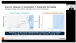
The biggest challenge in 2025 was managing rapid growth in design scale and system complexity, especially for AI-focused SoCs. Customers increasingly need high capacity, fast execution, and deep debug visibility at the same time. Verification has moved well beyond RTL correctness—teams are bringing up full systems with complex software stacks. This puts pressure on infrastructure while increasing sensitivity to cost, deployment effort, and workflow continuity. Tighter schedules and market uncertainty further pushed customers to look for platforms that can adapt across different development phases.

How is your company’s work addressing this challenge? 

A key issue we see is the trade-off between execution speed and debug depth. Traditionally, prototyping and emulation are handled by separate systems, which adds cost and slows iteration.

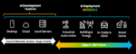
Our response has been to rethink how these needs are supported across a project’s lifecycle. With OmniDrive, we’re exploring a dual-mode approach built on a shared hardware foundation, allowing teams to use the same platform for fast software bring-up or deeper debug, depending on the stage of development. While the modes aren’t interchangeable at runtime, this approach helps reduce duplicated infrastructure and improve overall price-performance.

This direction is being refined through close collaboration with early customers, where we’re validating that it holds up in real engineering environments, both technically and economically.

What do you think the biggest growth area for 2026 will be, and why? How is your company’s work addressing this growth? 

We see RISC‑V and AI‑silicon as the key growth drivers in 2026. RISC‑V is moving into broader, more customized deployments, while AI workloads are drastically increasing design scale and complexity.

To support this, we provide a verification infrastructure built for scale. Our RTL Compile Flow (RCF) and Incremental Compile Flow (ICF) efficiently handle very large designs and are proven in multi‑FPGA deployments, shifting verification left.

In 2026, we will promote OmniDrive, our next‑generation emulation system. Based on latest FPGA architecture, its “dual‑mode” supports both emulation and prototyping, enabling high‑speed verification and fine‑grained debugging. This significantly reduces customer hardware investment and total cost.

Together, RCF, ICF, and OmniDrive offer a smooth progression from bring‑up to full‑system validation, helping customers scale while controlling both technical risk and infrastructure cost.

What conferences did you attend in 2025 and how was the traffic?

In 2025, we were selective about which conferences we attended and how much value they delivered. We’ve participated in DAC for many years, but this was the first year we chose not to attend. For us, DAC has become less effective in terms of qualified traffic and meaningful technical engagement, especially given how our customer base and focus areas have evolved.

In contrast, RISC-V–focused conferences, including Andes’ RISC-V CON and related ecosystem events, generated much more relevant and application-specific interaction. The audience there was closely aligned with what we’re working on—real systems, software bring-up, and system-level verification—so the conversations were more relevant and more actionable.

We also saw solid results from DVCon events across different regions. While traffic varied by location, the overall quality was strong, particularly among verification engineers and technical decision-makers. These events continue to be valuable for in-depth technical discussions rather than broad marketing exposure.

Overall, in 2025 we saw a clear shift away from large, general-purpose conferences toward more focused, domain-specific events. For us, relevance and engagement mattered far more than raw foot traffic, and that’s increasingly guiding where we invest our time.

Will you participate in conferences in 2026? Same or more as 2025?

We expect to remain active in industry conferences in 2026, at a similar level or slightly higher than in 2025. Our focus will continue to be on technically driven events that support deeper engineering discussion.

As SoC designs continue to scale up in size and complexity, we’ll place more emphasis on demonstrating how OmniDrive, together with our partitioning and RTL compile technologies, helps teams handle larger designs more efficiently. Rather than broad visibility, we prioritize venues where we can show practical system capability and engage with customers facing real scale and integration challenges.

How do customers normally engage with your company?

Customers usually first connect with us through events, press announcements, media coverage, advertising, or organic search. These initial touchpoints often spark technical conversations, such as system capacity, partitioning, or full-system bring-up challenges. From there, we work closely with engineering teams through evaluations, demos, and proof-of-concept projects. Given the scale and complexity of modern SoCs, these relationships tend to be long-term and collaborative, often spanning multiple design iterations. This approach ensures our engagements are practical, technically meaningful, and directly tied to customer needs.

Are you incorporating AI into your products? Is AI affecting the way you develop your products?

Yes, AI is starting to influence both our products and how we engage with customers. We’ve begun applying AI-driven techniques within our tool flows to help shorten compile time, reduce verification cycles, and improve performance efficiency in customer deployments.

At the same time, we’re preparing an AI-enabled knowledge base based on large models to support faster, more consistent technical guidance. While this capability is still being refined, the goal is to improve support efficiency without overcomplicating the engineering workflow.

Overall, we see AI as a practical enabler—used selectively to accelerate development and improve the customer experience in complex SoC and AI-driven designs.

Also Read:

S2C, MachineWare, and Andes Introduce RISC-V Co-Emulation Solution to Accelerate Chip Development

FPGA Prototyping in Practice: Addressing Peripheral Connectivity Challenges

S2C Advances RISC-V Ecosystem, Accelerating Innovation at 2025 Summit China

Double SoC prototyping performance with S2C’s VP1902-based S8-100


Arteris Smart NoC Automation: Accelerating AI-Ready SoC Design in the Era of Chiplets

Arteris Smart NoC Automation: Accelerating AI-Ready SoC Design in the Era of Chiplets
by Daniel Nenni on 01-22-2026 at 6:00 am

Smart NoC Automation Accelerating AI Ready SoC Design in the Era of Chiplet

Presentation from the 2025 SemiIsrael Expo

As semiconductor design pushes into increasingly complex territory, driven by Ai, ML, HPC, and heterogeneous system architectures, designers are challenged to balance performance, power, and time-to-market pressures. In this landscape, network-on-chip (NoC) architectures have emerged as a foundational building block for modern SoC interconnects, replacing traditional bus-based approaches to support scalable, high-bandwidth communication among numerous IP blocks. But designing an efficient NoC manually in an AI-ready SoC, especially with chiplet-based partitioning, quickly becomes a bottleneck. This is where Arteris Smart NoC Automation plays a transformative role.

Arteris Smart NoC Automation is a suite of tools and methodologies that automates the creation, optimization, and integration of NoC fabrics into SoC designs. Unlike conventional interconnect design flows that require extensive manual intervention, Smart NoC Automation uses intelligent, algorithm-driven processes to generate an interconnect tailored to the specific performance, throughput, latency, and area requirements of a given design. The result is a highly-optimized NoC that accelerates the path from specification to silicon, while ensuring that even the most demanding workloads, such as those driven by AI accelerators, are supported effectively.

At its core, Smart NoC Automation addresses the complexity of heterogeneous data flows within AI-ready SoCs. Modern AI workloads typically involve a diverse set of processing elements: CPUs, GPUs, AI accelerators, ISPs, and various memory subsystems (e.g., DDR, HBM). The communication patterns among these blocks are non-uniform and dynamic, requiring a flexible interconnect that can adapt to high-bandwidth data paths and low-latency control flows. Manual NoC design often results in over-provisioning (leading to wasted silicon) or under-provisioning (causing performance bottlenecks). Smart NoC Automation takes a data-driven approach, analyzing the specific traffic requirements of each block and producing a balanced network topology that meets performance goals with minimal overhead.

The transition to chiplet-based architectures further underscores the need for automated NoC design. Chiplet modular, pre-validated silicon blocks that are integrated into a system package using advanced interconnects (e.g., silicon interposers, organic substrates), enable designers to mix and match IP from different process nodes and vendors. While chiplets provide benefits such as improved yield and shorter development cycles, they complicate system integration: each chiplet may have distinct interface protocols, clock domains, and bandwidth profiles. Coordinating communication across chiplets demands a NoC fabric that can seamlessly bridge intra- and inter-chiplet domains, while maintaining coherence and meeting stringent latency constraints. Smart NoC Automation accelerates this by generating networks that are chiplet-aware, capable of mapping internal NoC segments to external interconnects with minimal designer effort.

Another key advantage of Smart NoC Automation is its ability to incorporate quality-of-service policies directly into the network fabric. AI workloads often have mixed-criticality traffic: real-time sensor data, high-volume tensor data streams, and control-plane signals all sharing the same network. Without QoS mechanisms, critical traffic can be delayed by bulk transfers, degrading performance and predictability. Automated NoC synthesis can embed traffic shaping, priority scheduling, and bandwidth reservation into the fabric, ensuring that performance-critical AI functions maintain determinism even under heavy load.

From a productivity standpoint, Smart NoC Automation drastically reduces design iterations. Traditional NoC design involves multiple manual tuning passes: adjusting topologies, re-evaluating performance models, and iterating physical design constraints. Automation compresses these cycles by generating optimized NoC proposals rapidly and enabling rapid what-if analyses. Designers can explore architectural alternatives and trade-offs interactively, without the lengthy turnaround times typically associated with manual RTL tweaking.

Finally, Smart NoC Automation supports hardware/software co-optimization, a crucial factor for AI-ready SoCs. By providing accurate performance models and exposing architectural parameters early in the design flow, software developers can optimize driver stacks, communication libraries, and scheduling algorithms in parallel with hardware development. This co-design approach ensures that both hardware and software are aligned for peak AI performance at launch.

Bottom line: Arteris Smart NoC Automation is a pivotal enabler for modern SoC design, especially in the era of AI and chiplets. By automating NoC generation and optimization, it removes one of the most time-consuming and error-prone steps in the SoC design flow, supports heterogeneous and chiplet-based architectures, ensures performance and QoS requirements are met, and accelerates overall time to silicon. As SoCs continue to scale in complexity to meet the demands of AI and next-generation compute workloads, Smart NoC Automation will remain essential for delivering high-performance, power-efficient designs on schedule.

Watch the full video here!

Contact Arteris

Also Read:

The IO Hub: An Emerging Pattern for System Connectivity in Chiplet-Based Designs

Arteris Simplifies Design Reuse with Magillem Packaging

Arteris Expands Their Multi-Die Support