Physical AI is changing how intelligent systems interact with the real world. These systems must sense, process, and respond to data in real time. Unlike cloud AI, Physical AI depends on fast local processing and reliable distributed communication. This shift creates a new challenge. Systems must move large volumes of sensor and control data quickly and predictably. Adaptive dataflow architectures address this challenge. They coordinate data movement across networks, compute platforms, and physical interfaces.
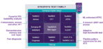
Three technologies play central roles in enabling these architectures: 25G Ethernet, PCIe 5.0, and multi-protocol PHYs. Together, they create a balanced connectivity foundation for Physical AI, Edge AI, 5G infrastructure, and Industry 4.0 deployments.
25G Ethernet: The Foundation for Distributed AI Data Movement
Physical AI systems generate massive amounts of data. Cameras, LiDAR, radar, machine vision systems, and industrial sensors continuously produce high-bandwidth streams. This data must move reliably between distributed compute nodes.
25G Ethernet provides the transport fabric that enables this communication. It delivers high throughput while maintaining low and predictable latency. These characteristics are critical for real-time decision systems.
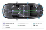
In autonomous vehicles, 25G Ethernet supports deterministic communication between sensors, domain controllers, and centralized compute units. In smart factories, it connects machine vision systems, robotics, and control platforms. In 5G networks, it supports fronthaul and midhaul data transport between radio units and baseband processing systems.
Another advantage of 25G Ethernet is scalability. It serves as a building block for higher-speed networking while maintaining strong power efficiency. This makes it well suited for distributed edge platforms that must balance performance and energy consumption.
While 25G Ethernet enables system-to-system data movement, internal compute platforms require equally efficient connectivity to process incoming data streams. This is where PCIe 5.0 plays a critical role.
PCIe 5.0: High-Performance Internal Connectivity for Edge Compute
PCIe 5.0 provides the internal data movement backbone within AI processing nodes. It connects CPUs, GPUs, AI accelerators, storage devices, and networking interfaces. These components must exchange data quickly to maintain real-time processing performance. Operating at 32 GT/s per lane, PCIe 5.0 doubles the bandwidth of PCIe 4.0. A full x16 configuration can deliver up to 128 GB/s of bidirectional throughput. This bandwidth supports demanding workloads such as sensor fusion, high-resolution video analytics, and real-time inference.
Although PCIe 6.0 exists, PCIe 5.0 remains highly relevant for edge deployments. It provides sufficient bandwidth for most inference and sensor processing workloads. At the same time, it avoids the higher power consumption and design complexity associated with newer signaling technologies.
Power efficiency is especially important for edge devices. PCIe 5.0 includes advanced power states that reduce energy consumption during idle or low-activity periods. Dynamic power gating helps minimize thermal load while maintaining system responsiveness. These features support automotive, industrial, and embedded AI platforms that operate under strict power constraints.
PCIe 5.0 also benefits from ecosystem maturity. Controllers, accelerators, and storage devices based on PCIe 5.0 are widely available and production-proven. This maturity improves interoperability and reduces integration risk. Designers can also optimize lane counts and channel configurations to balance bandwidth, area, and power.
While PCIe 5.0 enables high-speed data movement inside compute platforms and 25G Ethernet enables distributed communication, both rely on advanced physical signaling technologies. Multi-protocol PHYs provide this essential foundation.
Multi-Protocol PHY Architectures: Enabling Flexible Connectivity Convergence
Multi-protocol PHYs operate at the physical layer of high-speed communication systems. They provide the signaling infrastructure that enables reliable data transmission across electrical and optical channels.
Modern edge platforms often require support for multiple communication standards. These may include PCIe, Ethernet, CXL, and sensor interfaces such as JESD204. Multi-protocol PHYs allow these standards to share common SerDes resources.
This convergence reduces hardware complexity and improves silicon efficiency. It also allows systems to dynamically allocate high-speed I/O resources based on workload requirements. As Physical AI workloads evolve, platforms can adapt without major hardware redesign.
Multi-protocol PHYs also improve reliability. Advanced equalization, forward error correction, and clock recovery technologies help maintain signal integrity in harsh environments. These capabilities are essential for automotive, industrial, and telecom deployments.
Coordinating Adaptive Dataflow Across Distributed AI Systems
Adaptive dataflow architectures require synchronization across multiple connectivity layers. 25G Ethernet moves data between distributed systems. PCIe 5.0 enables high-speed communication within compute nodes. Multi-protocol PHYs ensure reliable signal transport across both domains.
Together, these technologies allow AI pipelines to operate with predictable latency and scalable bandwidth. They also improve overall system power efficiency by reducing redundant hardware and enabling flexible resource allocation.
Industry Impact
In automotive platforms, these technologies support distributed sensing, centralized AI processing, and deterministic vehicle networking. In Industry 4.0 environments, they enable real-time robotics coordination, machine vision analytics, and predictive maintenance. In 5G infrastructure, they support distributed radio processing and AI-driven network optimization.
Across these industries, adaptive dataflow architectures improve system responsiveness, scalability, and operational reliability.
Synopsys Solutions for Adaptive Dataflow Architectures
Physical AI systems depend on fast and reliable data movement. Adaptive dataflow architectures enable these systems to coordinate sensing, processing, and control in real time.
Beyond raw performance, long-lifecycle applications also demand proven reliability, functional safety, and security under harsh operating conditions. Features such as ASIL readiness and robust verification processes are essential for meeting these requirements across automotive, industrial, and 5G domains. Designers also benefit from solutions that integrate seamlessly across MAC, PCS, and PHY layers, reducing complexity and ensuring interoperability.
Synopsys’ portfolio of IP solutions include Ethernet, PCIe, multi-protocol PHYs with silicon-proven reliability and future-proofed for evolving connectivity standards. This creates a practical and power-efficient connectivity foundation for scalable next-generation edge intelligence platforms.
25G Ethernet PHY IP Performance Across PCIe 5.0 and 25GBASE-KR Modes
For more details, visit Synopsys IP for Edge AI.