You are currently viewing SemiWiki as a guest which gives you limited access to the site. To view blog comments and experience other SemiWiki features you must be a registered member. Registration is fast, simple, and absolutely free so please, join our community today!
In the late 1970s, cryptographic history saw the emergence of two seminal algorithms: McEliece and RSA. At that time, quantum threats were theoretical, and the selection criteria for cryptographic algorithms prioritized public key length and execution time, leading to RSA’s prominence while McEliece remained obscure despite its quantum-resistant properties. This changed in 1994 when Peter Shor’s algorithm exposed the vulnerabilities of both RSA and ECC to quantum attacks, sparking a quest for quantum-resistant cryptographic solutions. Since the early 2000s, the cryptographic community has pursued candidate algorithms to replace conventional standards, culminating in the National Institute of Standards and Technology (NIST) initiating a call for proposals in 2016 to establish Post-Quantum Cryptography (PQC) standards.
Why is PQC Important?
The impetus for PQC is multifaceted, anchored in the imminent reality of quantum computing. Unlike classical computers, quantum counterparts exhibit exponential growth in computational power, accelerating the potential breach of traditional cryptographic algorithms. PQC assumes paramount importance in safeguarding long-term confidentiality, preempting the specter of adversaries armed with powerful quantum computers poised to unravel encrypted communications. Standardization efforts, epitomized by initiatives like CNSA 2.0, underscore the strategic imperative of strengthening as soon as possible and even today cryptographic infrastructure against quantum adversaries of tomorrow.
Secure-IC, with years of experience in PQC implementation, offers a unique and empirical perspective on the challenges associated with transitioning from classic cryptography to PQC, including performance, security, and certification issues. In an upcoming webinar hosted by SemiWiki on Wednesday 19th June at 8AM PST / 5PM CET, Secure-IC’s co-founder and CTO, Sylvain Guilley, and CMO, Yan-Taro Clochard, will delve into the complexities of PQC adoption.
They will highlight the crucial importance of side-channel protection and the need for integrated hardware and software measures to ensure robust security. Additionally, they will discuss the intricate operation of PQC within integrated Secure Elements and showcase how Secure-IC’s Securyzr™ uniquely addresses these challenges.
The webinar agenda includes the following topics:
Why is transitioning to Post-Quantum Cryptography urgent for future security?
What are the key industrial challenges in implementing PQC?
How can side-channel protection enhance PQC security measures?
How do Secure-IC’s solutions ensure seamless and robust PQC implementation?
About Secure-IC
With presence and customers across 5 continents, Secure-IC is the rising leader and the only global provider of end-to-end cybersecurity solutions for embedded systems and connected objects.
Driven by a unique approach called PESC (Protect, Evaluate, Service & Certify), Secure-IC positions itself as a partner to support its clients throughout and beyond the IC design process. Relying on innovation and research activities, Secure-IC provides silicon-proven and cutting-edge protection technologies, integrated Secure Elements and security evaluation platforms to reach compliance with the highest level of certification for different markets (such as automotive & smart mobility, defense & space, semiconductors, critical infrastructures, server & cloud, healthcare, consumer electronics).
Securyzr™ global product range for Automotive (called Securyzr™ iSE_700 Series) is adapted for ISO 26262 and ISO/SAE 21434 requirements (with certified products up to ASIL-D) as well as to comply with security certification schemes in Automotive, such as Common Criteria EAL4+ PP0114 Car2Car (V2X). For more information, please visit https://www.secure-ic.com or follow Secure-IC on LinkedIn, X (Twitter), Wechat.
I recently had an eye-opening discussion regarding the phenomena of soft errors in semiconductor devices. I always knew this could be a problem in space, where there are all kinds of high energy particles. What I didn’t realize is there are two trends that are making this kind of problem relevant on the ground as well as in space. The combination of advanced processes and reliability-critical applications makes the problem very real in everyday settings. Think functional safety for autonomous vehicles, medical devices and high-performance compute clusters. In all these cases, the glitches that result from a single event upset (SEU) and the associated soft errors simply cannot be tolerated. Let’s explore how IROC makes the world a safer place with unique soft error analysis.
My Discussion
Dr. Issam Nofal
I had the good fortune of spending some time with Dr. Issam Nofal recently. Many thanks to Minji Lee, sales director at IROC for setting it up. Issam has been with IROC for over 23 years, literally since the beginning. He has held positions such as Product Manager, Project Leader, and R&D Engineer. He holds a PhD in Microelectronics from Grenoble INP and has been leading the company for the past two years. You can learn more about this unique company in an interview with Issam on SemiWiki here. You can also learn about the risks related to soft errors in this piece by Minji Lee on SemiWiki.
What I focused on in my discussion with Issam was how IROC finds and helps fix soft errors in many types of circuits with a unique tool called TFIT® (Transistor Failure In Time). Not only did Issam explain how the tool works and what makes it unique, he also provided a live demo. Issam is clearly a very technical CEO – he understands the company’s products and its customers very well.
What’s the Problem?
The first part of my discussion was to delve into why exotic high energy particle bombardment is a problem in everyday settings here on Earth. We already covered the reasons why the problem isn’t limited to devices in space. Advanced semiconductor processes make circuits more sensitive to soft errors and the growing use of these circuits in reliability-critical applications demands protection against glitches of all kinds.
So, exactly what happens to create issues at sea level? Issam explained that neutrons resulting from cosmic rays interacting with Earth’s atmosphere make it to ground level. Approximately 13 neutrons per square centimeter at sea level and the concentration increases with altitude. So why is this a problem? Issam explained that, while neutrons are not charged particles, they can still hit the atoms of the silicon. This can create an atomic reaction that creates secondary ionizing particles, like those we find in space. Those particles can cause problems. In addition, impurities in chip packaging materials can create alpha particles, which are ionizing and can cause upsets if they hit sensitive transistors.
So, there are potential particle interactions that can cause event upsets and soft errors all around us. At this point in the discussion the phrase you can run, but you can’t hide came to mind.
Finding and Fixing the Problem with TFIT
Analyzing designs for soft error sensitivity can be a daunting process. You can certainly bombard a device with high energy particles using specialized equipment and see what happens. While this can be useful, it is a post-production test that requires high cost and expertise. Also, post-production means repair of any issues found will require a re-spin.
Pre-fabrication analysis can be done with 3D TCAD simulations. While this provides useful information during the design phase, calibration and use of these tools in the typical design flow can be quite arduous, time consuming and error prone. The good news is there is a better way from IROC.
TFIT is a best-in-class transistor/cell level soft error simulator. IROC’s foundry partners develop models for TFIT based on an IROC-supplied methodology that uses simulation and calibrated measurements for a wide range of processes. Foundries also use the tool to optimize cell designs against soft errors. The TFIT methodology is based on foundry provided characterization models of ionizing particles for each technology node. These models are based on 3D TCAD simulations and actual measured effects of ionizing radiation from process test chips. The models are available for a range of process nodes from 65nm to N3 for TSMC, Samsung, GlobalFoundries, STM and IROC generic processes.
One of the unique features of TFIT is that it runs these models using a standard SPICE simulator. This facilitates much simpler setup and much faster run times, making sophisticated soft error analysis available to any design team working on cell libraries (IP) or a custom chip. The installation is straight-forward and Issam explained that new teams are up and running after one to two two-hour training sessions. Hspice, Eldo, Spectre, and Finesim are all supported.
TFIT essentially democratizes advanced soft error analysis, making this important optimization step available to all design teams. Issam shared the figure below to illustrate the TFIT flow.
TFIT Flow
Issam provided an overview of some of the main soft error analysis that is available with TFIT. The list is quite comprehensive:
Critical charge computation
Cross-section computation
Angular heavy ions impact simulation
Neutron SEU/SET FIT computation
Alpha particles accelerated testing simulation
Neutron MCU FIT and patterns computation
Thermal neutron SET/SEU computation
Issam then showed me how TFIT can be used to analyze design sensitivity to soft errors. The figure below shows how TFIT data can be overlaid on the actual circuit. What you see here is the areas of the design that are sensitive to particles of various energy levels, shown on the right side of the diagram as linear energy transfer (LET) values. Areas that are sensitive to lower energy particles are more likely to cause issues since lower energy particles are more likely to occur.
Armed with this kind of information, remediation can be added to the design to reduce sensitivity to soft errors. Issam explained that this typically takes the form of adding redundant copies of the sensitive circuits and using arbitration logic to monitor outputs to determine if a soft error occurs. In this case, the redundant logic can be used and circuit behavior is not interrupted. Note the separation of redundant circuits is also a consideration to ensure a soft error doesn’t impact more than one of the redundant circuit elements due to proximity.
The work involved here can be quite detailed. The good news is that TFIT is easy to use and runs fast so iterations can be done in a time and cost-efficient way.
Issam went on to show many more design techniques to reduce soft error sensitivity; approaches such as memory interleaving is one example. While the effort can seem large, the payoff is quite important. For the types of applications discussed, the interruption generated by soft errors cannot be tolerated. IROC has fast, easy to use tools, extensive experience and a broad set of foundry relationships to help you achieve this important goal efficiently.
The figure below illustrates the results of some of this work. In this case, the plot on the left shows significant areas of the circuit that are sensitive to high-energy particles. The plot on the right shows the results after layout optimization – with much smaller areas of sensitivity.
Layout Optimzation
To Learn More
If you are developing products for high-availability applications, getting to know how IROC can help you succeed is a must. You can find out more about the unique TFIT tool here. And that’s how IROC makes the world a safer place with unique soft error analysis.
The increasing demands of data-intensive applications necessitate more efficient storage and memory utilization. The rapid evolution of AI workloads, particularly with Generative AI (GenAI), demands infrastructure that can adapt to diverse computational needs. AI models vary widely in resource requirements, necessitating different optimization strategies for real-time and batch inference. Open infrastructure platforms, leveraging modular design and open standards, provide the flexibility to support various AI applications. Addressing scalability, performance bottlenecks, and continuous innovation are crucial for building systems that can handle the growing complexity and demands of AI workloads effectively.
Alphawave Semi recently sponsored a webinar on the topic of driving data frontiers using PCIe and CXL technologies with Dave Kulansky, Director of Product Marketing hosting the live session. Dave’s talk covered the motivation, the traditional and optical architectural configurations, the various components of the solution, the challenges with implementing optical interfaces and what kind of collaboration is needed for driving innovation.
Why PCIe and CXL for Driving Data Frontiers?
The evolution of PCIe (Peripheral Component Interconnect Express) and the advent of CXL (Compute Express Link) are pivotal in pushing the boundaries of data handling and processing in modern computing infrastructures. Designed to support high data transfer rates, PCIe and CXL enable rapid data movement essential for applications like AI/ML training, big data analytics, and real-time processing. PCIe’s scalable architecture and CXL’s enhanced functionality for coherent memory sharing and accelerator integration offer flexible system designs.
Both technologies prioritize power efficiency and robustness, with advanced error correction ensuring data integrity. CXL further enhances performance by reducing latency, enabling efficient memory utilization, and supporting virtualization and composable infrastructure, making these technologies indispensable for data-intensive and latency-sensitive applications.
Additionally, disaggregated infrastructure models, enabled by CXL’s low latency and high bandwidth, decouple compute, storage, and memory resources, allowing for modular scalability and optimized resource management. These advancements lead to enhanced performance and flexibility in data centers, high-performance computing, and cloud computing environments, ensuring efficient handling of dynamic workloads and large datasets while reducing operational costs.
Linear Pluggable Optics (LPO): A Key Advancement in High-Speed Networking
Linear Pluggable Optics (LPO) are crucial for meeting the escalating demands for higher bandwidth and efficiency in data centers and high-speed networking environments. LPO modules support data rates from 100 Gbps to 400 Gbps and beyond, leveraging PAM4 modulation to double data rates while maintaining power efficiency. Their pluggable form factor allows for easy integration and scalability, enabling network operators to upgrade systems with minimal disruption. LPO modules are compatible with a wide range of existing network hardware, ensuring seamless adoption. Their reliability and low latency make them ideal for data centers, telecommunications, cloud computing, and emerging technologies like AI and machine learning, providing a robust solution for evolving data transmission needs.
Energy-Efficient Accelerator Card
Energy-efficient solutions are key, particularly for data center networking, AI/ML workloads, and disaggregated infrastructure. An energy-efficient accelerator card, utilizing advanced electrical and optical interfaces, can significantly reduce power consumption while maintaining high performance. This card can integrate low-latency PCIe switches, potentially as optical interfaces, to enhance connectivity, support memory expansion, and optimize bandwidth.
The accelerator card approach offers scalability, resource efficiency, and accelerated processing, benefiting data centers and AI/ML applications by reducing energy costs and improving performance. Its hybrid electrical-optical design balances short-distance and long-distance data transfers, ensuring adaptability across various deployment scenarios. Smart power management and efficient thermal solutions further enhance its energy efficiency, making it a vital component for sustainable, scalable, and flexible computing environments.
Implementation Challenges
Implementing optical interfaces faces significant challenges, including the lack of standardization, nonlinearities of optical components, complexity in system-level analysis, and signal integrity optimization. Key issues include the absence of standardized optical interfaces from bodies like OIF and PCI-SIG, the nonlinear behavior of optical transmitters, the lack of comprehensive analysis tools for optical channels, and the need for optimized host setups and Continuous-Time Linear Equalization (CTLE) for signal integrity. Additional layer of complication is due to the fact that the original specifications were not anticipating current use cases, necessitating careful adaptation.
Addressing these challenges requires collaborative efforts to establish standards, advanced modeling and simulation tools, innovative signal processing techniques, and interdisciplinary collaboration.
Testing Approach
Transmitter dispersion and eye closure quaternary (TDECQ) and Bit Error Rate (BER) are important metrics for high performance in optical communication systems. An iterative testing approach can help refine optical interface implementations, ultimately leading to more efficient, reliable computing systems with enhanced connectivity. For example, first focus on minimizing TDECQ, adjusting transmitter (TX) settings such as laser bias, modulation current, pre-emphasis, de-emphasis, and pulse shaping, while maintaining optimal operating temperatures. Continuous monitoring and a feedback loop ensure these settings remain optimal.
Next focus on reducing BER, optimizing receiver (RX) settings including Clock and Data Recovery (CDR), Continuous-Time Linear Equalization (CTLE), Decision Feedback Equalization (DFE), Automatic Gain Control (AGC), and FIR filters.
Summary
Success hinges on ecosystem support, involving collaboration among stakeholders, standards bodies, and industry players to drive innovation.
Alphawave Semi collaborates with a broad range of industry bodies and players and its solutions deliver strong performance on various metrics.
Direct drive optical interconnects at 64Gbps appear feasible, offering a straightforward high-speed data transmission solution without retiming. However, scaling to 128Gbps may introduce signal integrity and timing challenges, potentially requiring retiming to ensure reliability. Navigating these challenges underscores the importance of coordinated efforts to balance practicality and performance as data rates rise.
The TSMC Technology Symposium provides a worldwide stage for TSMC to showcase its advanced technology impact and the extensive ecosystem that is part of the company’s vast reach. These events occur around the world and the schedule is winding down. TSMC covers many topics at its Technology Symposium, including industry-leading HPC, smartphone, IoT, and automotive platform solutions, 5nm, 4nm, 3nm, 2nm processes, ultra-low power, RF, embedded memory, power management, sensor technologies, and AI enablement. Capacity expansion and green manufacturing achievements were also discussed, along with TSMC’s Open Innovation Platform® ecosystem. These represent significant achievements for sure. For this post, I’d like to focus on another set of significant achievements in advanced packaging. This work has substantial implications for the future of the semiconductor industry. Let’s examine how TSMC advanced packaging overcomes the complexities of multi-die design.
Why Advanced Packaging is Important
Advanced packaging is a relatively new addition to the pure-play foundry model. It wasn’t all that long ago that packaging was a not-so-glamorous finishing requirement for a chip design that was outsourced to third parties. The design work was done by package engineers who got the final design thrown over the wall to fit into one of the standard package configurations. Today, package engineers are the rock stars of the design team. These folks are involved at the very beginning of the design and apply exotic materials and analysis tools to the project. The project isn’t real until the package engineer signs off that the design can indeed be assembled.
With this part of the design process becoming so critically important (and difficult) it’s no surprise that TSMC and other foundries stepped up to the challenge and made it part of the overall set of services provided. The driver for all this change can be traced back to three words: exponential complexity increase. For many years, exponential complexity increase was delivered by Moore’s Law in the form of larger and larger monolithic chips. Today, it takes more effort and cost to get to the next process node and when you finally get there the improvement isn’t as dramatic as it once was. On top of that, the size of new designs is so huge that it can’t fit on a single chip.
These trends have catalyzed a new era of exponential complexity increase, one that relies on heterogeneous integration of multiple dies (or chiplets) in a single package, and that has created the incredible focus and importance of advanced packaging as critical enabling technology. TSMC summarizes these trends nicely in the diagram below.
TSMC’s Advanced Packaging Technologies
TSMC presented many parts of its strategy to support advanced packaging and open the new era of heterogenous integration. These are the technology building blocks for TSMC’s 3DFabric™ Technology Portfolio:
CoWoS®: Chip-on-Wafer-on-Substrate is a 2.5D wafer-level multi-chip packaging technology that incorporates multiple dies side-by-side on a silicon interposer to achieve better interconnect density and performance. Individual chips are bonded through micro-bumps on a silicon interposer forming a chip-on-wafer (CoW).
InFO: Integrated Fan-Out wafer level packaging is a wafer level system integration technology platform, featuring high density RDL (Re-Distribution Layer) and TIV (Through InFO Via) for high-density interconnect and performance. The InFO platform offers various package schemes in 2D and 3D that are optimized for specific applications.
TSMC-SoIC®: Is a service platform that provides front-end, 3D inter-chip (3D IC) stacking technologies for re-integration of chiplets partitioned from a system on chip (SoC). The resulting integrated chip outperforms the original SoC in system performance. It also affords the flexibility to integrate additional system functionalities. The platform is fully compatible with CoWoS and InFO, offering a powerful “3Dx3D” system-level solution.
The figure below summarizes how the pieces fit together.
Getting all this to work across the ecosystem requires collaboration. To that end, TSMC has established the 3DFabric Alliance to enable work with 21 industry partners to cover memory, substrate, testing and OSAT collaborations to lower 3DIC design barriers, improve STCO and accelerate 3DIC adoption. The group also drives 3DIC development in tools, flows, IP, and interoperability for the entire 3Dfabric stack. The figure below summarizes the group of organizations that are involved in this work.
There is so much effort going on to support advanced packaging at TSMC. I will conclude with one more example of this work. 3Dblox™ is a standard new language that will help make designing 3D ICs much easier. TSMC created 3Dblox alongside its EDA partners such as Ansys, Cadence, Intel, Siemens, and Synopsys to unify the design ecosystem with qualified EDA tools and flows for TSMC 3DFabric technology. The figure below shows the progress that has been achieved with this effort.
3Dblox Roadmap
To Learn More
I have touched on only some of the great work going on at TSMC to create advanced packaging solutions to pave the way for the next era of multi-die, heterogeneous design. You can get more information about this important effort at TSMC here. And that’s how TSMC advanced packaging overcomes the complexities of multi-die design.
AI requires more Silicon capacity
Deep in the supply chain, some wizards turn sand into perfect diamond-structured crystal disks of silicon, which are necessary for the entire semiconductor supply chain.
They are part of the semiconductor supply chain, making Silicon Sand almost a thousand times more valuable.
The glimmer you see on the beach is Silicon. Silicon is a complex crystalline, brittle and solid metalloid (Metal and non-metal properties). Silicon is everywhere.
Behind oxygen, silicon is the 2nd most common material on Earth and the 7th most common material in the universe.
Silicon is a Semiconductor, which means it has electrical properties between a conductor (such as copper) and an insulator (such as glass).
A minute amount of foreign atoms in the silicon structure can radically change its behaviour, so semiconductor-grade silicon has to be incredibly pure. The lowest acceptable purity for electronic-grade silicon is 99.9999999%.
This means that only one non-silicon atom is allowed for every billion atoms.
Good drinking water allows for 4M non-water molecules, 500.000 times less pure than Semiconductor-Grade Silicon.
The blank wafer manufacturers must transform the High-Purity Silicon into a perfect Monocrystalline structure. This is done by introducing one single mother crystal into molten silicon at the right temperature. As new identical baby crystals start to grow around the mother crystal, the silicon ingot is slowly created out of the molten silicon.
This process is slow and can take up to a week. The finished ingot weighs in at around 100 kg and can create over 3,000 wafers.
A very thin diamond wire saws the silicon ingots into wafers two hair widths in size. The silicon-cutting tools are highly accurate, and the operators must be under constant supervision, or they will start using the tools to do silly things to their hair.
Hair of Silicon-cutting tool operator
This simple walkthrough of manufacturing blank wafers is criminally simplified and does not give sufficient credit to the wizards; it hopefully has provided a background for the dive into the blank wafer business.
Supply and demand in blank wafers
The blank wafer market is dominated by the four companies below. For long periods, the market has been in a delicate borderline capacity balance between supply and demand.
The dip in semiconductor sales in 2023 catapulted the market into oversupply, resulting in high internal and external inventories at chip manufacturers.
However, this is a temporary situation. As the market recovers, the industry will soon return to borderline capacity and must accommodate additional demand from the AI revolution.
The transformation from traditional CPU-based architectures to accelerated computing will impact the industry as it will require more silicon area than conventional architectures of the past.
Nvidia and TSMC will get the blank wafers they need, as the cost of the wafer compared to the total system cost is fractional. However, this could impact lower-value areas of the Semiconductor industry.
GPU architectures need more Silicon area.
As the hunger for performance increases, GPU manufacturers must battle several design limitations to extract more performance from their GPUs.
Making the die larger is an apparent way of getting higher performance, as electrons don’t like travelling long distances between different chips, which limits performance. However, there is a practical limit to how large it is possible to make the dies called the Reticle limit.
The reticle limit refers to the maximum size of a die that can be exposed in a single step on a photolithography machine used in semiconductor manufacturing. This limit is dictated by the maximum field size of the photolithography equipment, particularly the stepper or scanner used in the lithographic process. As of recent technology, the reticle limit is typically around 858 mm².
This size limitation is significant because it determines the maximum area that can be patterned on a wafer in one exposure. If a die is larger than this limit, multiple exposures would be required to fully pattern the die, which is impractical for high-volume manufacturing due to complexity and alignment challenges.
The new GB200 will overcome this limit by combining two reticle-limited dies on a silicon interposer, creating a super die 2x the reticle limit.
The other performance limitations are the amount of memory and the distance to it (translates into memory bandwidth). The new GPU architectures overcome this by using stacked High Bandwith Memory mounted on the same silicon interposer as the two GPU dies.
The problem with HBM from a silicon perspective is that the silicon area per bit is 2x traditional DRAM due to the highly parallel interface needed to create the high bandwidth. HBM also incorporated a logic control die in each stack, adding to the silicon area.
A rough calculation shows that a 2.5D GPU architecture uses 2.5x to 3x the silicon area that a traditional 2.0D architecture would use.
As was seen earlier, the blank wafer capacity will likely be very tight again unless the wafer companies are ready for this change.
The future capacity of the blank wafer market
The first of three laws of semiconductor manufacturing states that you need to invest the most when you have the least. This is due to the industry’s cyclical nature, which is very hard for semiconductor companies to follow.
As can be seen below, most of the blank wafer manufacturers are aware of the impact of this change, and the combined quarterly Capex has ballooned by almost threefold over the last few quarters. This is despite the difficult market conditions faced by the blank wafer companies.
What is even more interesting is that this trend started a long time ago. The blank wafer companies got lucky or knew something others did not.
The Semiconductor supply chain is a Time Machine that can predict future things. Your future might be somebody else’s past. While we don’t always get answers, we almost always get questions worth interrogating.
Dan is joined by Mark Himelstein, President of Heavenstone. Most recently, as Chief Technology Officer at RISC-V International, Mark contributed to shaping RISC-V technology through visionary leadership and industry expertise. He has a track record of executive roles at Graphite Systems, Quantum, and Infoblox.
Dan discusses the RISC-V community with Mark with a specific focus on the importance of software and how it provides the backbone for collaboration across the industry. The result is accelerated innovation across many markets and applications.
Mark also discusses the upcoming RISC-V event hosted by Andes Technology, Deep Dive into Automotive/AI/Application Processors and Security Trends. The event will take place on June 11th, 2024 from 9:30 AM – 5:00 PM at the DoubleTree by Hilton Hotel in San Jose.
Mark will be moderating an ecosystem panel at the event entitled Unlocking the RISC-V Application Processor Potential. Representatives from Andes, Google, OSYX Technologies, and RISE will participate. Mark also discusses how to get involved in the RISC-V movement.
The views, thoughts, and opinions expressed in these podcasts belong solely to the speaker, and not to the speaker’s employer, organization, committee or any other group or individual.
In the fast-paced world of Electronic Design Automation (EDA), the complexity of chip designs is continuously rising. With the burgeoning of systems such as 5G communication devices and Advanced Driver-Assistance Systems (ADAS) teeming with thousands of components, the demand for robust and efficient prototyping platforms is more critical than ever.
Evolving Challenges in FPGA Prototyping
Continued semiconductor industry growth depends on delivering ever more complex chip designs, co-verified with specialized system software – in less time with relatively fewer mistakes. Traditional FPGA chips, limited by their logic units and memory capacity, are often insufficient for the needs of modern applications. Furthermore, the array of interfaces and IP cores, including PCIe, USB, MIPI, and LPDDR, introduces significant complexity to system integration, which requires prototyping platforms proficient at adjusting changing standards and ensuring seamless integration of hardware and software components.
As SoC designs grow increasingly intricate, traditional partitioning software often fails to maximize FPGA resource utilization. With the demand for large-scale chip designs to be segmented into numerous parts—often as many as 64 or even 128 individual FPGA units—and the presence of more complex system topologies, there’s a pressing need for software tools that are both cost-effective and user-friendly, adeptly meeting the modern chip architecture’s evolving requirements. Moreover, optimizing human resource allocation, minimizing bring-up time, and streamlining the debugging process are crucial for boosting the efficiency and pace of the development workflow.
S2C FPGA Prototyping Solution
Confronted with these challenges, S2C Prototyping Solutions emerged as a trusted ally, offering a streamlined pathway for verification and demonstration, empowering developers to amplify the unique value propositions of their SoCs.
Automated Design Partitioning:
S2C offers a comprehensive suite of tools that facilitate and enhance design verification. The Prodigy PlayerPro, a highly automated solution engineered to perform intricate partitioning tasks using sophisticated algorithms without manual oversight, optimizes FPGA resource allocation and minimizes inter-FPGA signal latency. This significantly improves the success rates of FPGA placement and routing. Enhanced with FDC constraint-based partitioning and automated I/O assignment, PlayerPro efficiently streamlines the prototyping workflow, substantially reducing bring-up times and accelerating iterative development through ECO Flow.
Industry-leading Performance:
S2C’s Prodigy Prototyping Solution leverages advanced TDM Aware technology to optimize Time Division Multiplexing (TDM) ratios based on timing criticality, ensuring each system meets the highest performance benchmarks. This capability is augmented by system-level Static Timing Analysis (SSTA), which proactively identifies and mitigates potential performance bottlenecks early in the design phase, significantly boosting the efficiency and outcome of projects.
Robust and Stable Platform:
Engineered for high performance and uniformity, the S2C Prodigy Prototyping platform is underpinned by rigorous production process oversight, stringent quality control standards, and robust supply chain capabilities. This solid foundation guarantees dependable and consistent outcomes, crucial for the success of product development.
Comprehensive Solutions:
To address the diverse needs of the industry, S2C offers an extensive range of peripherals and reference designs. With over 90+ ready-to-use daughter cards, PCIe5 Speed Adapters, Memory DFI PHYs, and ChipLink IP solutions, S2C ensures that all aspects of system integration are covered, providing exceptional performance, and simplifying the entire design and verification process.
With over 20+ years of industry experience and a relentless commitment to innovation, S2C equips clients with highly trusted tools necessary to stay ahead in the competitive market. Our solutions accelerate the time-to-market successfully, delivering unparalleled speed, accuracy, and dependability.
Dieter Therssen obtained his master’s degree in Electronics Engineering from KU Leuven in 1987. He started his career as a hardware design engineer, using IMEC’s visionary tools and design methodologies in the early days of silicon integration.
Since then, Dieter developed his career across many digital technologies, in a broad range of applications and for a variety of companies. He’s been development manager of the International Technology Center Leuven; led the Audio Competence Center at Philips Semiconductors in Nijmegen; co-founded NXP software and Beatbrew; was Director for European automotive business at Premium Sound Solutions 2011, later transitioning its electronics business into Lear Corporation; and directed DSP Valley, an independent cluster of digital companies in the Low Countries.
Being CEO of Sigasi, a fast-growing, creative technology company in a B2B setting, is a perfect fit for Dieter. Having worked in that space for several companies, and well-rooted in the field of semiconductors, Dieter forever enjoys the magic of a motivated team.
Tell us about Sigasi.
Sigasi is redefining hardware description language (HDL) creation, integration, and validation in the digital design specification world. Our driving force is the shift-left principle: instilling the importance of catching potential errors and issues in specifications as early as possible in the design cycle.
HDL has long been created by talented designers writing code in simple environments, which they then need to slowly check manually, or rely on teams further down the line to point out errors. Sigasi is here to improve this onerous, laborious hardware design workflow. Why not create HDL specifications much more smoothly, integrate various time-saving methodologies and tools into the work, and validate code before it throws monkey wrenches into the simulation and synthesis flows, or the physical implementation flow? Sigasi makes all this possible.
In terms of the industry, Sigasi sits at the intersection of HDL creation and its hand-off to the down-stream EDA workflow. As a digital chip design verification company, we help hardware designers focus on their design content because our Integrated Design Environment (IDE) verifies their code as they’re typing or importing it.
What is the Shift-Left Methodology?
To understand Shift Left, it’s best to understand how hardware—and perhaps software designers—depict the flow of a design moving from a concept to a real chip. That starts at the left-hand side of the drawing board and ends up at the right-hand side.
On the right side, picture chips lying on a desk or sitting on a PCB and being tested. Think of architects that come up with how to solve this real-world problem in one way or another. Moving from one side to the other, hardware designs go through a lot of steps, a lot of transformations. Fixing a problem as it occurs later in the chain costs outrageously more than fixing it at the start of the process.
Harry Foster at Siemens has shown how costly mistakes can be in the chip design flow.
Costly mistakes can upend a chip design project. Source: Harry Foster, Siemens
It’s shocking to see that the magnitude of cost involved on the left-hand side of the picture, as opposed to the right-hand side, is a factor of 40,000. That’s the magnitude of cost involved in undoing errors. Catch them at the beginning and pay 40,000 times less than if they are caught at the end.
Essentially, we’re talking about the principle that catching errors much earlier in the design can save a lot of money, certainly when compared to catching them towards the end of the design. Shifting left prevents costly mistakes and makes hardware design more efficient from the start.
What problems is Sigasi solving?
For more than 60 years, we have seen semiconductor manufacturers going to smaller nodes, bigger wafers, stretching lithography to the EUV spectrum, deploying more efficient materials, and even changing the implementation of the transistor, with FinFET and GAA as the latest incarnations. As a result, those manufacturers are offering enough real estate to put 200-billion transistors on a chip.
What is often forgotten is that designs still need to be created with that same capacity. That is the EDA world. Designers ultimately create layout files that manufacturers use to start their implementation process. The transformation of the layout files into lithography masks is after all the first step in the manufacturing process. Therefore, tools leading to the creation of those layout files also need to keep changing to keep up with capacity and the ever-changing physical manifestations that impact performance, power, and area (PPA). And that starts with the specification of an FPGA, ASIC, or SoC application.
What application areas are Sigasi’s strongest?
Any market that efficiently deploys artificial intelligence (AI) introduces complexity and uncertainty into the front-end design flow. Advantages of AI in the medical world result in better ways to perform and analyze MRIs, CTs, X-rays, EKGs, and other tests. This opens the door for new, AI-deploying chip designs. Sigasi offers the guardrails needed to resolve the uncertainty of AI creativity, with a deterministic validation flow.
The Race for Space is creating competition for exploration, homeland security, communication, and such is leading to opportunities worldwide to create satellites filled with AI-powered ICs. Design complexity is challenging. Another is the automotive sector where Advanced Driver-Assistance systems (ADAS) combined with sophisticated infotainment and hybrid engines has led to an explosion of Electronic Control Units (ECU) needed for cars. A hybrid SUV has more than 100 ECUs. This complexity goes beyond the cognitive abilities of most humans. Sigasi offers the organization that is now essential to designing the ICs for such complex systems.
Whether a company makes one or a million chips a year for space applications, they still need to be designed—free of errors.
What keeps Sigasi’s customers up at night?
HDL designers worry about complexity and the need to manage all the risks. Even an expert HDL coder can’t keep track of all the requirements for an appropriate coding style. Safety measures, security vulnerabilities, and PPA constraints impose rules and measures that need to be addressed in HDL ahead of hand off.
A designer’s nightmares are full of missed deadlines and schedule slips, cost overruns, falling short of goals, writing poor test benches, HDL design integrity so the specification must correspond to intent. Verification methodologies such as UVM ease writing good test benches, yet another worry added to the broad check-box list. Integrating HDL leads to mixing SystemVerilog and VHDL when the ideal library or IP might not be available in the preferred hardware design language.
The nightmare scenarios are endless.
What does the competitive landscape look like and how does Sigasi differentiate?
Many linting tools are commercially available. It takes time before they work their way through the design, compile it and come up with feedback for the user, which is typically verbose. They do a great job, of course, but they do catch errors on a delay. Designs need to be finished and free of syntax errors before you can run them.
Our differentiation is our shift-left approach. Our tools are upfront and real-time. We incrementally compile the entire design with every stroke of a keyboard, which is fundamentally different from what the other tools do.
Moreover, we are unique in how our solutions don’t just offer users an information dump, but rather give focused, relevant feedback. When building our tools, Sigasi engineers think about whether a problem could be the consequence of a preceding problem, and how it might be more efficient to report only the first problem, since fixing it will also fix the other problem. That is how we compile a succinct summary of what is wrong with the design. Our engine understands the semantics of SystemVerilog and VHDL. It is not just an editor or spell check. It understands how these languages work and what different combinations could mean—ensuring a hardware engineer gets fast, germane reporting.
What new features/technology is Sigasi working on?
We’re putting the finishing touches on an updated product portfolio and hierarchy of product offerings. Expanding our product lines will help individual designers verify their code and entire groups ensure their projects are on track and doing what they should do without constantly making changes.
SemiWiki readers can expect more of the software world’s best practices in Sigasi’s products, going beyond our shift-left approach. For example, we’ll be introducing our command language interface (CLI), which is essential for the automation of any workflow. But it certainly comes in handy for continuous integration/continuous deployment (CI/CD)––a concept borrowed from the software world, where it’s customary for engineers to work in agile ways––that looks at the entire main code repository.
How do customers normally engage with Sigasi?
Our website is sigasi.com. Sigasi can be reached by e-mail at info@sigasi.com. We’re also on LinkedIn @company/sigasi/.
We’ll also be at DAC flying our new logo and tagline “Put Your Semicolons to Work” while exhibiting its Sigasi Visual HDL at DAC Booth #2416 (second floor).
At the recent User2user conference, Amit Kumar, Principal Hardware Engineer, Microsoft, shared the company’s experience from building a 3DIC SoC and highlighted Siemens EDA tools that were used. The following is a synthesis of core aspects of that talk.
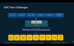
3DIC Challenges
Despite the numerous advantages of 3DIC technology, its adoption is accompanied by several challenges. These include higher overall system costs, lower yield for the whole system, increased power density and thermal management difficulties, design complexity, Through-Silicon Vias (TSV) overhead, timing variation uncertainties, the need for new testing and verification methods, hierarchical and modular design requirements, and a lack of standards. Addressing these challenges requires collaborative efforts from industry stakeholders to develop innovative solutions, adopt best practices, and establish industry standards, ultimately unlocking the full potential of 3DIC technology for next-generation electronic systems.
3DIC Flow & Data Management Challenges
3DICs introduce a host of challenges, particularly in design flow and data management. Integrating heterogeneous technologies and managing complex interconnections across multiple layers demand robust data management solutions and comprehensive verification methodologies. Ensuring design integrity and reliability while navigating the intricate 3DIC landscape requires meticulous attention to detail and innovative approaches to data handling.
TSMC 3DBlox Open Standard
The 3DBlox technology is an open-source standard and promotes interoperability and collaboration across the semiconductor industry. TSMC’s 3DBlox 1.0 laid the foundation for 3D integration, enabling designers to stack logic and memory dies with TSVs for improved performance and power efficiency. Building upon this foundation, TSMC unveiled 3DBlox 2.0, further enhancing the scalability and flexibility of 3DIC designs with advanced packaging options and improved interconnect technologies. This includes ability to stack chips manufactured on different process nodes, enabling heterogeneous integration and maximizing design flexibility.
Design, Physical Verification, Reliability Analysis for 3DIC
Designing a 3DIC involves a multifaceted process encompassing design, physical verification, and reliability analysis. Designers must meticulously craft layouts that optimize performance, minimize power consumption, and ensure compatibility with heterogeneous technologies. Physical verification and reliability analysis are equally critical, encompassing checks for Design Rule Violations (DRV), Layout versus Schematic (LVS) verification, and reliability assessments such as thermal analysis and electromigration checks.
3DIC Verification Flow
Microbump libraries and Power Delivery Network (PDN) delivery are crucial for efficient signal routing and power distribution in 3DIC design. Microbump libraries offer optimized configurations for inter-die connections, while PDN delivery ensures robust power distribution for high-performance 3DICs. Verification at the die, package, and interposer levels is vital for seamless integration. Die-level verification ensures compliance and reliability, while package and interposer verification validate system integrity, covering signal, thermal, and mechanical aspects. The verification flow includes standalone verification of package-interposer layers, integrated verification, and staged approaches for early issue identification and resolution, ensuring the integrity and reliability of 3DIC designs.
Physical Verification Using Siemens EDA Tools
Verification using Siemens XSI (Xpedition Substrate Integrator) and Calibre 3DSTACK together offer a comprehensive solution for validating the integrity, functionality, and manufacturability of 3DIC designs. These tools leverage heterogeneous data sources, including ODB++, GDS, OASIS, LEF/DEF, and Verilog formats, to build a full system model encompassing all components and layers of the 3DIC design. They generate system-level netlists suitable for Layout vs. Schematic (LVS) and Static Timing Analysis (STA), enabling comprehensive verification of connectivity and timing characteristics. With support for detailed connectivity visualization, device transformation, and creation of interconnected devices, XSI and Calibre 3DSTACK facilitate the seamless integration and validation of 3DIC designs, ensuring successful development and deployment of high-performance and reliable solutions.
Calibre 3DSTACK
Calibre 3DSTACK is essential for verifying the integrity of stacked dies in 3DIC design. It utilizes data from XSI and specific physical details to configure checks for design rules and connectivity. The tool offers a range of checks, focusing on port and text attributes, which users can customize based on their requirements. By detecting issues like floating texts and verifying port connectivity, Calibre 3DSTACK ensures the reliability and manufacturability of 3DIC designs. It integrates seamlessly with XSI, enabling accurate verification and analysis for high-performance 3DIC solutions.
XSI Utilities and Automation
XSI simplifies 3DIC design projects with its utilities and automation features. It enables project database creation, data extraction, and setup propagation for efficient project management. The tool’s bump file splitting utility categorizes bump data, while automatic text identification and alignment streamline text manipulation. Property propagation ensures consistency, and runset creation automates connectivity checks, enhancing verification efficiency. These capabilities enhance productivity and accuracy in 3DIC design workflows, leading to optimal results in design and verification.
Optical Shrink and Thermal Expansion Handling
Optical shrink and thermal expansion pose unique challenges in 3DIC design, necessitating specialized methodologies and tools for accurate modeling. Optical shrink refers to feature distortion during lithography, while thermal expansion affects stacked die stability. XSI and Calibre 3DSTACK support die shrinking and optical shrink, ensuring functionality while reducing feature sizes. Verification tools address die shrinking mismatches, ensuring proper alignment and connectivity between stacked dies. Thermal expansion coefficients are considered to predict and mitigate package expansion effects. Thermal mechanical analysis evaluates thermal expansion impact on 3DIC stack integrity.
Summary
The journey towards realizing the full potential of 3DIC technology is marked by challenges and opportunities. From data management and design flow challenges to physical verification and reliability analysis, each aspect of 3DIC design demands meticulous attention and innovative solutions. By leveraging cutting-edge tools and methodologies, designers can navigate the complexities of 3DIC design and unlock new possibilities for high-performance and compact electronic systems. Siemens EDA is working closely across the ecosystem to deliver cutting edge tools and methodologies that support multi-vendor flow.
Establishing void-free fill of high aspect ratio TSVs, capped by a thin and uniform bulk layer optimized for removal by CMP, means fully optimizing each of a series of critical phases. As we will see in this 3-part series, the conditions governing outcomes for each phase vary greatly, and the complexity of interacting factors means that starting from scratch poses an empirical pursuit that is expensive and of long duration.
Robust and void-free filling of TSVs with copper progresses through six phases as laid out below:
Feature wetting and wafer entry (previous article)
Feature polarization
Nucleation
Fill propagation
Accelerator ejection
Bulk layer plating
(Rinsing and drying, which we won’t cover in this series)
Fill Propagation
Ok, so, now that we’ve reached the third part of this 3 part series about TSV fill, we get to talk about the fill part of TSV fill.
We wetted the features completely and our dwell step ensured that copper cations and accelerator molecules were able to gather in the bottom of the via. We initiated a potential on the system, driving a current that causes copper deposition to begin. If our via sidewall (especially low down) was characterized by significant roughness, we spiked that current density to get an even initiation of deposition. All that’s left is to let fill happen. Right?
Well, actually…yeah, largely that should be right. If we chose a good chemistry and we were careful in setting up polarization, confirming the initiation of bottom up fill through FIB/SEM inspection, the fill “should” go as planned.
Here’s where we see the delicate interaction of our organic additives at play. Suppressor, coating the upper wall of the via (as well as the entire surface of the wafer), increases the over-potential required to reduce the ions to metallic copper. Meanwhile, accelerator is adsorbed in concentration on the via floor and to some degree slightly up the via sidewall near the bottom. And, whereas the suppressor is busy making it harder for copper cations to be reduced, the accelerator is making it easier. Current is flowing, and, because in copper plating the plating efficiency approaches 100%, each electron that passes takes part in the reduction of copper ions and thus the formation of copper metal. Thus copper deposition is happening and it is happening in the one place where we made it easiest. The via bottom.
We have flipped the physics on its head.
A few interesting things happen now. As we shared, it takes real time for a cupric ion to diffuse to the via bottom. In the case of a 10X100 micron via, it may take as much as 5 seconds!! Thus the current density must be kept high enough to plate at a useful rate but low enough to avoid consuming the ions faster than they can diffuse down from the top of the via. Technically, it is possible to work a model to estimate this rate. Trial and error works too if you have access to wafers and inspection.
It’s time for a meaningful aside here.
First, it is not necessary to commit an entire wafer to each TSV fill test you run. TSV wafers can be cleaved into pieces (we typically call them coupons) and fill can be optimized by running the tests on the individual coupons. This saves a LOT of wafers. A coupon 4cm X 4cm would suffice. At this size (depending on feature layouts) you could possibly cleave 7 or 8 coupons from a 150mm TSV wafer and as many as 18 from a 200mm. That’s a lot more tests!
There are some tricks to successfully mounting and plating coupons and the supplies that make it easy are readily found in online stores like Amazon. If interested to learn more, hit us up at info@techsovereignpartners.com.
Once you’ve gotten fill optimized on coupons, transferring the recipe to a full wafer is all about scaling the current to maintain the current density (pay close attention to the actual open area of the wafer); and making sure deposition rates are equal across the wafer diameter. Cross-wafer uniformity establishment is a topic all on its own not only applicable in TSV fill but in plating generally; we won’t cover in today’s discussion.
That’s it for our aside, back to propagation of fill. Superconformal deposition, i.e. fill, is happening. The sidewall copper of the via is staying thin but the bottom is getting thicker. If it is not, and instead deposition is conformal (happening on both sidewalls and bottom) or sub-conformal (happening really only on the walls and not the bottom), then there are two likely root cause possibilities (and both may be at play).
Before we explore root causes, let’s talk about how one determines whether super conformal fill is happening in the first place. As we said, and you likely already know, TSV fill can be a long process step, even an hour or more. FIB/SEM is a quite indispensable means of inspection for determining the performance of fill. But even the FIB cut can take a long, long time and FIB time is expensive. For these reasons and more, we recommend that, when working to optimize fill, you do not attempt to fill the entire via. Aim, instead, for a 1/4 or 1/3 fill, i.e. a partial fill. This makes each test go much faster and the FIB cuts faster too. More importantly, though, it shows you with clarity whether superconformal fill is happening or not. As we said in the previous article, if you did not get polarization right in the beginning, no recipe adjustment is going to fix it. Continue optimizing through imaging of partially filled vias until you confirm that copper growth is minimal or undetectable on the upper sidewalls and robust on the bottom.
Figure 1. Partial Fill of 10X100 micron via. Images courtesy ClassOne Technology
Meanwhile, back to root causes when this is not evident. As stated, we likely have two. They are:
The current setpoint is not optimal.
The additive ratios are not optimal.
First, current setpoint. Here’s a dirty little secret about “setting current”. You are actually setting potential (voltage). The cell (electrolyte, hardware of the reactor and the wafer itself) then determine a current based on that potential. Ideally, the power supply you use does allow a current setpoint but what it is actually doing is aiming for a potential that it expects will produce your target current, and adjusting based on ammeter output to settle on target. But there’s more, it isn’t really current you are after; it’s current density. And now, the geometry, size and count of vias plays a direct part in converting that current into a current density. Your chemistry vendor ideally has provided you with a target current density, from which you can calculate a target current based on the dimensions and number of vias on your wafer. If no target current density is provided, you’ve bought a ticket on the DOE express and you have some work to do.
Second is the additive ratios. Really, your chemistry vendor has almost certainly provided you with target additive ratios based on their own studies. You are certainly welcome to perform your early optimization tests by varying these ratios, however we would recommend trusting those ratios at the start. Crafting and executing a DOE around just current setpoints will be time consuming already. Adding a second parameter will of course greatly expand the test set, but including additive ratio tests also means dumping and re-pouring the bath again and again. Again, the chemistry vendor has likely determined an optimal ratio of additives. If they have not, or you have a via of highly non-standard dimensions, you may not be able to escape additive ratio testing.
So, through attentive preparation and testing, you established good bottom up fill, as verified by FIB/SEM imaging. In other words, the floor of the via is rising. This is exciting and you deserve a drink. But don’t forget, you were only doing partial fills so you are actually not done at all.
There are a few effects of this rising floor phenomenon. First, accelerator, generally speaking, does not get integrated into the plated copper, meaning that it continues to “ride the floor” as the via fills. Any accelerator adsorbed to the lower sidewalls is now getting swept up and added to the accelerator on the floor, increasing the concentration further. Incidentally, sidewall suppressor is getting displaced along the way. Acceleration is accelerating, in a sense. Fill may be moving faster in terms of vertical growth. That’s nice for throughput.
The other thing that’s happening is that the long, long time it was taking for copper ions to get down to the via bottom is getting shorter and shorter because the via is getting shorter and shorter. Your high aspect ratio via is becoming a moderate to low aspect ratio via. So this means, if throughput matters to you, you can make edit the recipe such that it starts as a “high aspect ratio via” recipe and modulates to a “moderate” and finally “low aspect ratio via” recipe. You can run what we’d commonly call a stair-step recipe. Which means that, at the start of fill, we use a relatively low current that maintains good fill (based on the current density recommended by your chemistry vendor and your via dimension calculations), then at some point later, when the via is shorter (for a 10X100micron via maybe a quarter shorter) the current can be stepped up higher. And then again later, and then again. Don’t get me wrong, fill “should” progress fine without stepping up the current. But faster is better. A stair-step recipe well constructed should fill a 10X100 micron via in under an hour. Without the stair-step, this fill time can be much, much longer.
Figure 2. Fully Filled 10×100 micron via (FIB/SEM). Image courtesy of ClassOne Technology
Figure 2. Fully Filled 10×100 micron via (FIB/SEM). Image courtesy of ClassOne Technology
Accelerator Ejection
Ok the via floor is approaching the top! This is great news. Unless you forgot about the brakes. Remember, we basically super charged the via floor with spicy, spicy accelerator molecules. They’re doing their job and that via floor is rushing up to the top of the hole. We’d like it to conveniently stop, pretty please, immediately at the top. But will it? In fact, it will not without proper attention and mounds will form above the vias, creating major problems in CMP, typically leaving un-polished copper bumps over every via. This is of course a no go for subsequent steps in the integration.
So what to do about it. The easy button is to, well, not get cheap when selecting a TSV chemistry. Chemical displacement is your friend when it comes to accelerator ejection and the avoidance of forming copper humps above your vias. A carefully and properly formulated leveler polymer is key here. In advanced TSV chemistries, the leveler magically ejects the accelerator as it reaches the top of the via hole. Easy.
Ok, what if your TSV chemistry works fine but doesn’t do the magic ejection thing? There is still a solution for you. You can force the ejection of ALL additives from all surfaces of what is now essentially a flat, copper coated wafer with no holes in it. Doing so requires two things: the right timing and the right power supply. First timing: You need to know when, in your recipe, the copper has reached the top of the hole. Again this can be done in coupon testing for recipe optimization. At the point when copper has reached the top, you can introduce a reverse pulse of the power supply in your recipe. Hence the second point, you would need the right power supply. A supply that is capable to pulse is very valuable in copper plating. A power supply that can pulse with a forward potential (one that deposits copper onto the wafer) and can also pulse with a reverse potential (one that removes copper from a wafer) provides even more flexibility.
Introducing a brief pulse in reverse will cause all additives to eject from the entire wafer surface. The step can be very short because the ejection is nearly instantaneous. We would recommend a short step, perhaps 50 milliseconds, and for simplicity we would recommend using the initial current at the beginning of your fill (not the high current nucleation step). Now you’ll return to forward potential for the bulk layer plating and additive adsorption will be what it will be; you don’t really care because the entire surface will see the same species adsorption now that the advantages associated with tall via holes is eliminated.
Figure 4. Oblique view of final bulk layer film (SEM). Image courtesy of ClassOne Technology
Bulk Layer Plating
Vias are filled. There were no voids. Well, you hope there’s no voids. I’m not sure you really checked every via. Anyway, you also ejected all that accelerator you worked so hard to adsorb (sigh). And now you need a layer of sacrificial copper on top of it all so that the CMP folk can polish it back to leave a perfectly flat hybrid surface of silicon perforated by neat little copper circles belying tall and slender, buried pillars of pristine copper.
Well, generally speaking, you can crank that power supply up now. As long as you’ve established good cross-wafer plating rate uniformity, you can go as fast as the chemistry can keep up with. 40 amps on a 300mm wafer is legitimate with most TSV chemistries. We can do the math. That’s about 18 amp on a 200mm wafer and 10 amp on a 150mm wafer.
So, you’re good at this and that film is very uniform. The question is, how thick do you make it? The answer is, I don’t really know for sure, sorry. For that you’ll have to talk to your CMP people. CMP, of course, takes advantage of insitu uniformity tracking and can make closed loop adjustments to maintain uniform removal. Exactly how quickly a uniform polish can be established depends on the optimization and the capabilities of that tool set. Obviously, CMP is one of the more expensive unit processes in the fab and financial controllers and fab managers will be interested to keep those costs as low as is practical. No, they’ll probably want costs lower than practical but that’s why they hired you. So, this means keeping that film as thin as possible, both from the plating perspective (maintaining uniformity) and the CMP perspective (uniform polish). That sounds like more DOE work. I hope you’ve looked up what “DOE” means by now.
If you have questions about TSV fill or some of the sub-topics raised in these articles, do reach out at info@techsovereignpartners.com