Up to now the RISC-V community has been developing open-source processor implementations to a stage where they can appeal to system designers looking for alternatives to proprietary Arm and x86 cores. Toward this end, two projects have emerged as particularly significant examples of where RISC-V is heading. One is Ara, a vector processor developed at ETH Zürich as part of the PULP platform. A second is XiangShan, a high-performance scalar core developed in China. Both are serious engineering efforts. Both are open source. Yet they represent fundamentally different answers to the same question: how should RISC-V scale performance?
Ara Takes the Explicit Vector Path
Ara implements the RISC-V Vector Extension by making parallelism explicit to software. The design exposes vector width, register grouping, and data locality directly to the programmer. Software controls how many elements execute in parallel through VL, how wide those elements are via SEW, and how registers are grouped using LMUL. Memory behavior remains visible and largely software managed.
The key architectural decision in Ara is the elimination of speculation. Rather than attempting to discover parallelism dynamically in hardware, Ara requires software to declare it explicitly. Because the work is explicitly structured, there is no branch speculation inside vector loops, no instruction reordering speculation, no guessing about memory dependencies, and no need for rollback mechanisms. Ara executes exactly the work it is instructed to execute.
This distinction matters for performance analysis. A stall is simply waiting for data to arrive. A speculative penalty is wasted execution followed by recovery. Ara still pays for memory latency, but it never flushes pipelines, squashes instructions, replays large instruction windows, or discards completed work.
“Ara was designed to prioritize efficiency for highly parallel workloads rather than speculative general-purpose execution. By eliminating speculation in the vector engine, we avoid the energy cost of mispredictions and pipeline recovery, allowing the hardware to focus almost entirely on productive computation. For large, structured workloads such as matrix multiplication, this approach consistently delivers very high functional-unit utilization and strong performance-per-watt,” says Matteo Perotti, ETH Zürich.
Ara’s vector model makes this non-speculative execution practical. Vector instructions amortize control overhead across many elements. Loop bounds and memory access patterns are regular. Control flow is largely outside the hot loop, and data dependencies are explicit. That structure eliminates the need for speculation to keep pipelines busy.
A Shallow Memory Hierarchy
Ara’s memory system reinforces this philosophy. Unlike conventional CPUs or GPUs, Ara does not include private L1 caches for vector execution. Its load-store unit connects directly to a shared SRAM-based last-level memory. Depending on the integration context, this memory may act as a cache, a software-managed scratchpad, or a preloaded working set.
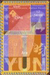
In simulation, Ara is exercised in a bare-metal environment where data is preloaded into memory to accelerate simulation runtime. Full operating-system bring-up and debugging are performed directly on FPGA platforms where execution speed makes system-level validation practical. In ASIC prototypes such as Yun, the last-level memory appears as a small on-chip SRAM. In FPGA integrations such as Cheshire, Ara is integrated into a full SoC with operating-system support.
What remains consistent across these systems is the architectural intent: locality is a software responsibility, not something to be speculatively optimized away by deep cache hierarchies. This approach aligns closely with RVV’s execution model. Vector performance depends less on hiding latency than on sustaining bandwidth and reuse.
Where Vectors Begin to Strain
Ara is also instructive because it reveals where vector architectures begin to strain. Matrix-dominated workloads, now central to AI and machine learning, can be expressed on vector engines through careful tiling and accumulation. Ara demonstrates that this can be done effectively, but not without increasing register pressure, instruction overhead, and software complexity.
Rather than masking these challenges with additional hardware, Ara exposes them cleanly. In doing so, it helps explain why the RISC-V ecosystem is now exploring matrix extensions as a distinct architectural layer above vectors. Ara effectively defines the upper bound of what pure vector execution can deliver, making it a valuable reference point rather than an endpoint, as illustrated by AraXL’s large-scale vector implementations.
XiangShan Takes the Traditional Path
By way of comparison, XiangShan follows the traditional high-performance CPU path. The project refines speculative scalar execution to extract instruction-level parallelism from largely unstructured code. Its design relies on deep out-of-order pipelines, aggressive branch prediction, speculative memory access, and multi-level caching to infer parallelism dynamically and hide latency behind hardware complexity.
Performance emerges when predictions are correct, and the cost of being wrong is absorbed through rollback, replay, and wasted energy. XiangShan must speculate because scalar code is dominated by frequent branches, irregular memory access, fine-grained dependencies, and unpredictable control flow. Speculation is the only way to extract performance from that environment.
This approach is familiar, effective for general-purpose workloads, and deliberately conservative. XiangShan aims to demonstrate that an open RISC-V core can compete by mastering the same techniques long used by x86 and Arm processors. The trade-off is therefore not one of right versus wrong, but of where complexity lives: XiangShan concentrates complexity in hardware to preserve the illusion of fast sequential execution, while Ara moves structure into software and removes speculative machinery entirely.
The Commercialization Question
Unlike Ara, which is best understood as a reference and research platform, XiangShan occupies a more ambiguous space between research and industry. XiangShan is not owned or sold by a commercial IP vendor in the traditional sense. There is no company marketing XiangShan cores under paid licensing terms. Instead, the project’s RTL is released under the Mulan PSL v2 open-source license, allowing companies to adopt, modify, and integrate the design without royalties.
However, XiangShan has progressed well beyond academia. The project has produced multiple physical tape-outs across successive generations, including chips fabricated in both mature and more advanced process nodes. Systems are capable of booting Linux and running standard benchmarks. Project materials describe collaboration with industry partners and evaluation within SoC development workflows.
This places XiangShan in a Linux-like model of commercialization. The core itself is not monetized as proprietary IP. Instead, its value emerges through adoption, integration, and downstream products built by third parties. In other words, XiangShan has been commercialized in practice, but not in the conventional IP-licensing sense. Its success depends on whether companies choose to build products around it, rather than on direct sales of the core itself.
XiangShan succeeds in demonstrating that open-source hardware can scale to complex, production-class microarchitectures. Its investment in tooling, simulation, and verification shows that openness need not imply fragility. In that respect, it validates RISC-V as a viable foundation for serious scalar CPUs.
At the same time, XiangShan’s conservatism defines its limits. By adhering closely to the speculative scalar tradition refined by x86 and Arm, it avoids questioning the underlying assumptions of that model. It does not attempt to make parallelism explicit, to rethink locality management, or to reduce reliance on speculation as the primary driver of performance. XiangShan improves the state of the art within a familiar framework but does not attempt to redraw that framework.
Two Paths, Not One Winner
Comparing Ara and XiangShan is illuminating precisely because they are not competing for the same point in design space. Ara explores explicit, structured parallelism and predictable performance, scaling by adding lanes, bandwidth, and disciplined data reuse. XiangShan refines speculative scalar execution, scaling by increasing pipeline sophistication, prediction accuracy, and cache depth. One exposes trade-offs to software. The other works hard to hide them. One favors determinism. The other embraces speculation. Neither approach is inherently superior, but each excels in different domains.
What Open Source Means in Practice
Earlier analysis of XiangShan made the case that open source alone does not guarantee architectural boldness. Ara reinforces the complementary point: architectural boldness does not require commercial polish to be meaningful. Ara’s value lies in clarity. It shows what RVV actually implies when implemented honestly, including both its strengths and its limits. XiangShan’s value lies in execution discipline and scale. It shows how far open source can go by perfecting known techniques and coupling them with institutional support.
Together, these projects illustrate the breadth of architectural exploration now possible within the RISC-V ecosystem. One path is evolutionary and production-oriented. The other is exploratory and architectural. Understanding both is essential for anyone trying to anticipate where RISC-V and high-performance computing more broadly is headed next.
Also Read:
The Launch of RISC-V Now! A New Chapter in Open Computing
The Foundry Model Is Morphing — Again
SiFive to Power Next-Gen RISC-V AI Data Centers with NVIDIA NVLink Fusion