Despite a severe setback, Nvidia pulled it off once again
There have been serious concerns about the ROI on AI and yield problems with Blackwell, but Nvidia pulled it off again and delivered a result significantly above guidance.
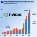
Beating the revenue guidance of $28B with 2B$ to just above 30B$, representing 15% QoQ and a 122% YoY growth. As usual, the increase was driven by the Data Centre business that reached $26.3B, demonstrating that the H100 is not just filling the void before Blackwell takes over, but the H100 demand is still solid.
Despite the excellent result and a mixture of “Maintain” and “Outperform” ratings from the analyst communities, the investor community was less impressed, and the Nvidia stock responded negatively.
It looks like the worry of some of the larger financial institutions and economists about AI’s ROI has taken hold, and investors are starting to believe in it. What I know for sure is that I know as much about AI’s future return as anybody else: Nothing!
Mark Zuckerberg of Meta formulated it well when dividing the Meta AI investment into two buckets: a practical AI investment with very tangible returns and a more speculative long-term generative AI investment.
As I have lived through the dot-com crash of the early millennium, I know that a fairy tale is only a fairy tale when you choose the right moment to end the story. Many stocks that tanked and rightfully were seen as bubble stocks are with us today and incredibly valuable. I had shares in a small graphic company that tanked during that period – fortunately, I kept the shares or else I would not have been able to write this article. It is too early to tell how the AI revolution will end, but companies are still willing to invest (bet) in AI.
Not surprisingly, the analyst community was interested in Jensen Huang’s view of this, and he was very willing to attack the likely most significant growth inhibitor of the Nvidia stock.
While I will not comment on the stock price, I believe Jensen did an excellent job framing the company’s growth thesis. Opposed to how critics have presented it, it is not only a question of AI ROI—it should be seen in the much larger frame of Accelerated computing.
Without being too specific on the actual numbers and growth rates, Jensen presented his growth thesis based on the combined value of the current traditional data centre on a round of $1T.
While we can be criticised for working without exact numbers, we believe that viewing research on a high level with approximate numbers can provide value if you have a large-scale impact that does not require precision to provide insight. Fortunately, this is the foundation of any Nvidia analysis at the moment.
It is possible to judge if the 1T$ datacenter value is reasonable. The Property Plant and Equipment value (PPE) of the top 5 data centre owners is above 650B$, and the same companies have a depreciation of 28B$; the rough average write-off period is 5.8 years, suggesting the PPE is heavy on Server equipment with 4-5 year write off periods.
The 1T$ value is a reasonable approximation for the Nvidia growth thesis.
This is what we extracted from Nvidia’s investor call and would frame as Nvidia’s growth thesis:
Nvidia is at a tipping point between traditional CPU-based computing and GPU-based accelerated computing in the data center, and Blackwell represents a step function in this tipping point. In other words – you ain’t seen anything yet!
The fertile lands for Nvidia’s GPUs are not only the new fields of AI but also the existing and well-established data centres of today. They will also have to convert their workloads to accelerated computing for cost, power and efficiency reasons.
The current depreciation of the 1T data center value we calculate to 43B$/quarter, in other words, this is what is needed to maintain the value of the existing data centres. This depreciation is likely going to increase if Nvidia’s growth thesis is right that the data centers will have to convert their existing capacity to accelerated computing.
The current results of Nvidia will pale in comparison with the post-Blackwell era.
A prediction is not a result, but Jensen did an excellent job of framing the opportunity into a very tangible $1T+ opportunity and a more speculative xxxB$ AI opportunity that shows that Nvidia is not opportunity-limited. There is plenty of room to grow into a very tangible market.
It is time to dive into the details.
The status of Nvidia’s business
Investigating the product perspective, the GPU business dominates but both the Software and Networking products also did well.
From a quarterly perspective, software outgrew the rest with 27% growth while GPU took the price from a YoY perspective with 130% growth followed by 100% network growth and 70% software growth. We already know that Nvidia has transformed from a component to a systems company but the next transformation to services could be in sight. This reveals that Nvidia’s moat is more than serves and that it is expanding.
From a Data center platform perspective, this was expected to be the Blackwell quarter but no meaningful revenue was recorded.
The revenue is completely dominated by the H100 platform while the A100 is close to being phased out. The Chinese revenue kept growing at a strong rate despite having been setback by the restrictions imposed by the US government on GPU sales to China. We categorise all the architectures allowed in China (A800 and H800) as H20 (specially designed for China).
While Nvidia’s revenue by country can be hard to decipher as it is a mixture of direct and indirect business through integrators, the China business is purely based on what is billed in China.
As can be seen, the China revenue is showing strong growth. In the last quarter it grew by more than 47% bringing revenue back to close to the pre embargo period. Nvidia highlighted that China is a highly competitive market (lower prices) for AI but it is obvious that Nvidia competes well in China.
This is also a strong indication of the market position of Nvidia, even in a low cost market bound by embargoes, Nvidia’s competitive power is incredibly strong.
The increased GPU revenue is not really showing in the CapEx of the known cloud owners in China. We will continue following this topic over time.
The systems perspective
With AMD’s acquisition of ZT Systems accelerating the company’s journey from a components to a systems company, it is worth analysing Nvidia with that lens.
Nvidia have already made this transition back in Q3-23 when the first H100 revenue became visible.
Onwards the revenue is no more concentrated around Nvidia silicon (GPU+Network) but also memory silicon from predominantly SK Hynix and an increasing “Other” category that represent the systems transformation.
The other category also includes the advanced packaging including the still very costly built up substrates necessary for H100 and later for Blackwell.
This demonstrates that while the ZT Systems makes AMD more competitive, the company is not overtaking Nvidia but catching up to a similar level of competitiveness from a systems perspective.
The Q3 result in more detail
As can be seen from the chart, there was significant growth in Nvidias revenue, Gross margin and operating margin but not to the same degree as the last couple of quarters.
The growth rates are declining and this is a cause for concern in the analyst community and likely the reason the stock market response has been less than ecstatic.
Indeed the quarterly revenue growth rate was down from 17.8% last quarter to 15% this quarter and both Gross Profit Margin an Operating Profit Margin declined. In isolation this looks like the brakes are slightly impacting the Nvidia hypergrowth. Numbers don’t lie but they always exist in a context that seems to have eluded the analyst community
3 Months ago, Jensen Huang declared that there would be a lot of Blackwell revenue in both the quarter and the rest of the year but shortly after a design flaw allegedly impacting yields was found and a metal mask layer of Blackwell had to be reworked. In reality a key growth component vaporised and should have left the quarter in ruins. Nevertheless Nvidia delivered a result just shy of the growth performance of the last few stellar quarters.
Knowing how complex the semiconductor supply chain is, this is a testament to Nvidia’s operational agility and ability to deliver. The company did not get sufficient credit for this.
A dive into the supply machine room can add to the story.
The supply machine room
Assuming that the Q2 Cost of Goods Sold represent a balanced (under continuous steep growth) Nvidia requires 215K$ worth of COGS to generate 1B$ in revenue. The Q3-24 increase in revenue represent and additional COGS of 860K$ bringing the total COGS needed to 6.5B$
The COGS grew to 7.5B$ while the inventory also accelerated its increase from 600K$/qtr to 800$/qtr.
In total the COGS/Inventory position grew by 1-1.2B$ above of what Nvidia would need to deliver the result in H100 Terms. This represent the impact of the unexpected problems with Blackwell.
In other terms, Nvidia was probably preparing for around 5B$ worth of Blackwell revenue that now had to be replaced with H100 revenue.
Simultaneously, the TSMC HPC revenue jumped in what could be caused by other customers but also undoubtedly some extra work for Nvidia based on the Blackwell issues.
As seen on the TSMC HPC revenue, it also took a bump of 2.2B$, which easily can contain the 1-1.2B$ additional COGS/Inventory that Nvidia is exhibiting.
No matter what, the Blackwell issue was significant and Nvidia delt with it without taking the credit but downplaying the issues in the investor call. From my experience working in semiconductors battleships, this was like a direct hit close to the ammunition stores and everybody has been in panic. On the outside and on the investor call, this was treated like a gracing blow.
Demand and Competition
Rightfully a good analysis should include the competitive situation and a view on the demand side of the equation. We recently covered those two areas in the article: OMG It’s alive. The conclusion of that article is that Nvidias competitive advantage remains strong and that the CapEx of the large cloud providers are growing in line with their cloud businesses. The visibility of CapEx spend is also favorable to Nvidia and the AI companies in general.
Conclusion
As always, we do not try and predict any share price but concentrate on the underlying business results. Sometimes the two are connected, other times not.
This analysis shows that Nvidia pulled of a very good result while the company took a direct hit to the hull. The impact of the Blackwell issue was significant but handled with some damage to revenue growth and profitability. This will likely recover soon.
It reconfirmed Nvidia’s journey towards a systems company with strong networking and software growth and an increase in CapEx could signal something interesting is brewing. While the AMD ZT Systems acquisition is good for the company, it does not represent a tangible threat to Nvidia
The H100 platform is executing impressively and now accounts for 19B$/Qtr or 73% of the DC business and more than 63% of the total Nvidia revenue. Despite Blackwell problems, the H100 supply chain pulled through and Nvidia blew through the 28B$ guidance.
China is becoming important again with strong growth of over 47% QoQ. The Chinese share of revenue is now back to more than 12% of total revenue. Nvidia has clearly struck a balance between cost and performance that does not hurt the profitability of the company. While it is not visible where the GPU goes, it is safe to assume the Chinese growth does not stop here.
For us the most interesting thing in the Nvidia call was the revelation of the Nvidia Growth Thesis (our term) as a response to the worries of ROI on AI spread by banks and economists based on short term returns. We think that Jensen Huang layed out an excellent growth thesis with plenty of opportunity to grow while at the same time addressing the ROI on AI.
A more pressing issue will be the ROI on the $1T traditional CPU based data center value that will depreciate with $43B (our analysis) per quarter. Jensen argues that this will not be able to compete with accelerated computing and will be unable to compete very soon.
If Jensen is right here, there is no need to worry about the ROI on AI for some time. The cloud companies will have to invest just to protect their cloud business.
It looks like the growth thesis has escaped the most of the analyst community that are more interested in calculating the next quarter than lifting their gaze to the horizon. The future looks bright for Nvidia.
While our ambition is to stay neutral, we allow ourselves to be impressed every once in a while and that is what we were in this investor call.
Pledge your support for this content
Also Read:
Robust Semiconductor Market in 2024
Semiconductor CapEx Down in 2024, Up Strongly in 2025
Automotive Semiconductor Market Slowing


