RVN! 26 Banner revised (800 x 100 px) (600 x 100 px)

EDA and ITC

EDA and ITC
by Daniel Payne on 10-17-2011 at 10:44 am

Every SOC that is designed must be tested and the premier conference for test is ITC, held last month in Anaheim, California.

I spoke with Robert Ruiz of Synopsys by phone on September 21st to get an update on what is new with EDA for test engineers this year. Robert and I first met back at Viewlogic when Sunrise was acquired in the 90’s.

The Big Picture
Over the years Synopsys has built and acquired a full lineup of EDA tools for test and they call it synthesis-based test:

Scan Test is a very well known technique and designers can choose either full-scan or partial-scan using the TetraMAX tool (technology initially acquired from Sunrise).

The STAR Memory System is technology acquired from Virage and it is well received in the industry with some 1 billion chips containing this IP to date.

Test engineers have a few choices with EDA tools, either buy from one vendor or from multiple vendors where you stitch the point tools together:

Questions and Answers
Q: With smaller process nodes there is more chance for Single Event Upset (SEU) in memories. How do you design for that?
A: SEU is mitigated by using Error Correcting Coding at the design stage.

Q: BIST is a popular test approach, but how do you know that your test electronics is OK?
A: The test electronics is treated like other parts of the logic design, and we add it to the scan chain too.

Q: Where would I use your Yield Analysis tool?
A: Within a foundry for example on the initial yield of new nodes there may be low yield, so this approach helps them find out where on each design the yield is being limited.

Q: Who else would use Yield Analysis?
A: We see users in IDM, Foundries and Fabless wanting to improve yield with this tool.

Q: How does static timing analysis work with ATPG?
A: In our test flow Static Timing Analysis (Prime Time) can guide TetraMAX (ATPG) for critical paths and area defects. Slack info sent to TetraMAX that will uncover any timing defects.

Q: Do temperature gradients cause speed faults?
A: Yes, and you could uncover any speed fault with our tools.

Q: What kind of Market share does Synopsys have in the EDA test tools?
A: Mentor and Synopsys are the top two suppliers for DFT tools. The top 20 semi companies roughly split in DFT between SNPS and MENT.

Q: Was Mentor Graphics the first to offer compression tools for test?
A: Yes, however our compression is more efficient compared to their approach.

Q: How are Synopsys test tools different from Mentor or Cadence tools?
A: The design flow using our logic synthesis is the biggest difference. For Memory and IO testing we lead in this IP (through Virage).

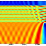
Q: Can scan compression create routing issues like congestion?
A: Yes, here’s a graphical comparison of routing congestion – white and red are high congestion in routing. Optimization for removing congestion is shown on the right-hand side. At synthesis stage any congestion will make the physical design tool run times much longer, or even fail to complete. Smart synthesis tools can help on congestion so that P&R times are quicker.

Q: What kind of industry endorsements do your DFT tools have?
A: We’re in the TSMC Reference flows.

Q: What are some pitfalls during test?
A: During test your chip may draw more power than in the budget (red is too much power), and that can damage the device during scan testing. Users can define their power budget during testing using DFT tools (green shows the budget), lower power can mean longer run times. This is a mature technology and it doesn’t require extra DFT up front (DFTMAX has compression).


SIG feedback – 19[SUP]th[/SUP] annual event this past Monday, tech papers presented. Samsung presented in 2010 for reduced tester power consumption.

Q: What’s happened after the Virage acquisition?
Q: Synopsys had a relationship with Virage before acquisition. Now the DFT tools know the scan chains and can connect memory scan to logic scan more efficiently. We can even re-use shift registers as scan elements, saving area up to 10% based on design style.

We can model memories with scan chains embedded, then optimize the ATPG runtimes. Use the Virage memories and Synopsys ATPG for the best test results.

Q: How do I optimize the number of scan chains?
A: Our tools let you optimize that.

Q: What is Yield Explorer all about?
A: This tool reads silicon data that is failing scan tests.

  • – Accept physical design info and know where the defect is occurring (this via, that cell)
  • – Also useful for volume diagnosis.
  • – Defects today can be subtle, beyond just stuck-at faults, more cross-talk induced errors or noise errors.


This can help get to a higher yield quicker. Use the defective silicon data to help diagnose and pinpoint where to find failures. Create a candidate list of where to look. Designers can become more involved on where the failures are located at.

Q: How can you find and then verify IC defects?
A: Use etching techniques to find it visually. Yield analysis will pinpoint to the cell level what is suspect.

Q: Who is using this Yield Analysis capability?
Q: One customer is ST Ericsson who presented at SIG on Monday, they ran the Yield Explorer with TetraMAX and immediately found a via causing loss. They then made one design change, and yield went up 47%. They used the LEF/DEF feature to reduce area to look for loss. Fewer scripts to glue tools together.

Q: Yervant Zorian, tell me about Virage within Synopsys now.

A: We started 10 years ago to offer Memory test automation, and are now in our 4[SUP]th[/SUP] generation of memory test with some 1 billion chips using the Virage approach. The percentage of SOCs using RAM can be 60% now, so memory yield can limit the chip yield. Power is an issue during the testing of RAMs so you have to be intelligent about how to test these without exceeding limits.

In our IP with BIST the DFT tools used by the designer can analyze the results all the way down to the physical level.

The diagnosis of chips through JTAG ports allow the debug of all memories on the SOC in a low-cost fashion.

One challenge is how to diagnose SRAMs early in a new node that is just being defined. With Yield Analysis you can now use an automated approach to help improve yield for this.

All of our memory IP requires extensive characterization before it gets placed in a new SOC.

Summary
Synopsys offers a full suite of DFT tools and testable IP used by both design engineers and test engineers. The dominance of Design Compiler for logic synthesis is what makes the Synopsys tools different from the other vendor offerings.


TSMC Gets Fooled Again!

TSMC Gets Fooled Again!
by Daniel Nenni on 10-16-2011 at 2:51 pm

If you follow the SemiWiki Twitter feed you may have noticed that The Motley Fool (Seth Jayson) did three more articles on TSMC financials. The first Foolish article was blogged on SemiWiki as “TSMC Financial Status and OIP Update”.

The next three Fool Hardy articles look at cash flow (the cash moving in and out of a business), accounts receivable (AR), days sales outstanding (DSO) and a closer look at margins. All three articles are interesting reads so if you have the time I would definitely click over. If not, here are the cool pictures and my expert guess of the foundry business going forward.
Don’t Get Too Worked Up Over #TSMCEarnings http://www.fool.com/investing/general/2011/10/04/dont-get-too-worked-up-over-taiwan-semiconductor-.aspx

Over the past 12 months, Taiwan Semiconductor Manufacturing generated $687.4 million cash while it booked net income of $5,543.0 million. That means it turned 4.5% of its revenue into FCF (Free Cash Flow). That sounds OK.

However, FCF is less than net income. Ideally, we’d like to see the opposite. Since a single-company snapshot doesn’t offer much context, it always pays to compare that figure to sector and industry peers and competitors, to see how your business stacks up.

With questionable cash flows amounting to only -1.1% of operating cash flow, Taiwan Semiconductor Manufacturing’s cash flows look clean. Within the questionable cash flow figure plotted in the TTM period above, changes in taxes payable provided the biggest boost, at 1% of cash flow from operations. Overall, the biggest drag on FCF came from capital expenditures, which consumed 92.2% of cash from operations.

DanielNenni SemiWiki.com
#TSMCPasses This Key Test fool.com/investing/gene…

Sometimes, problems with AR or DSO simply indicate a change in the business (like an acquisition), or lax collections. However, AR that grows more quickly than revenue, or ballooning DSO, can also suggest a desperate company that’s trying to boost sales by giving its customers overly generous payment terms. Alternately, it can indicate that the company sprinted to book a load of sales at the end of the quarter, like used-car dealers on the 29th of the month. (Sometimes, companies do both.)

Why might an upstanding firm like Taiwan Semiconductor Manufacturing do this? For the same reason any other company might: to make the numbers. Investors don’t like revenue shortfalls, and employees don’t like reporting them to their superiors.

Is Taiwan Semiconductor Manufacturing sending any potential warning signs? Take a look at the chart above, which plots revenue growth against AR growth, and DSO. Will Taiwan Semiconductor Manufacturing miss its numbers in the next quarter or two? I don’t think so. AR and DSO look healthy. For the last fully reported fiscal quarter, Taiwan Semiconductor Manufacturing’s year-over-year revenue grew 5.3%, and its AR dropped 3.9%. That looks OK. End-of-quarter DSO decreased 8.7% from the prior-year quarter. It was down 4.9% versus the prior quarter.
DanielNenni SemiWiki.com
Are You Watching This Trend at #TSMC? fool.com/investing/gene…

Margins matter. The more Taiwan Semiconductor Manufacturing (NYSE: TSM ) keeps of each buck it earns in revenue, the more money it has to invest in growth, fund new strategic plans, or (gasp!) distribute to shareholders. Healthy margins often separate pretenders from the best stocks in the market. That’s why we check up on margins at least once a quarter in this series. I’m looking for the absolute numbers, comparisons to sector peers and competitors, and any trend that may tell me how strong Taiwan Semiconductor Manufacturing’s competitive position could be.

Here’s the margin picture for Taiwan Semiconductor Manufacturing over the past few years:

Here’s how the stats break down:

  • Over the past five years, gross margin peaked at 49.4% and averaged 45.8%. Operating margin peaked at 40.1% and averaged 35%. Net margin peaked at 40% and averaged 34.5%.
  • TTM gross margin is 48.7%, 290 basis points better than the five-year average. TTM operating margin is 36.9%, 190 basis points better than the five-year average. TTM net margin is 36.5%, 200 basis points better than the five-year average.

With recent TTM operating margins exceeding historical averages, Taiwan Semiconductor Manufacturing looks like it is doing fine.

My expert guess is that the semiconductor industry will continue to struggle as a result of the economic uncertainty around the world. Unemployment, debt, housing crisis, over population (7 Billion+ people!); consumers will spend less money on electronics next year. To make things worse, semiconductor inventories are at pre-recession levels. In Q2 2011, the DOI (days of inventory) reached 83.4 days, exceeding the last record high of 83.1 days seen in the first quarter of 2008. The good news is that smart phones are no longer considered a luxury, smart phones are now life lines which means they will continue to hyper drive the semiconductor industry for years to come. China is hugely subsidizing mobile phones and India launched a $35 tablet ($60 cost) so the internet will be coming before indoor plumbing in some regions.

In regards to TSMC, it is all good news. Take a look at the charts and you will see an extremely healthy company in a VERY competitive market and the MOST economically challenging times the semiconductor industry has ever seen. TSMC has already won the 28nm node and 20nm is not far behind. TSMC is easily a $20 stock, believe it.

UMC botched 40nm and is struggling with 28nm, this really breaks my heart as I absolutely respect the UMC engineers. SMIC was a huge disappointment. Backed by the Chinese government and the largest domestic market for consumer electronics, how could they fail? But fail they did. Hopefully the recent re-org will get SMIC back in the foundry game! I also had high hopes for GlobalFoundries as a competitive threat for TSMC. GFI is actually doing quite well, unfortunately we all got carried away in the excitement and unachievable expectations were set. Intel 22nm may be the only real threat to TSMC at 28nm and it will certainly be exciting to see how that all plays out.


Austin and San Jose SCC

Austin and San Jose SCC
by Paul McLellan on 10-14-2011 at 3:35 pm

Don’t forget the SpringSoft Community Conferences next week in Austin on Tuesday and in San Jose on Thursday. There is no charge and you even get a free lunch (see “no such thing as…”).

The morning in Austin is focused on functional closure and how to leverage SpringSoft’s verification technology around Verdi and Certitude and the new ProtoLink Probe Visualizer for FPGA debug. The afternoon is focused on custom IC design and how to get better results using the Laker custom IC technology.

In San Jose this order is reversed, with the morning being dedicated to custom IC design and the afternoon to functional verification.

Registration for both SCC conferences is here.


Soft IP Qualification

Soft IP Qualification
by Paul McLellan on 10-14-2011 at 3:10 pm

At the TSMC Open Innovation Platform Ecosystem Forum (try saying that three times in a row) next week (on Tuesday 18th), Atrenta will present a paper on the TSMC soft IP qualification flow. It will be presented by Anuj Kumar, senior manager of the customer consulting group.

More and more, chips are not put together what we think of as the standard way, by writing a bunch of RTL and then going through “classic” EDA. Instead, they are assembled out of pre-existing IP, either from the 3rd party IP marketplace or from a previous chip in the same company. So the focus of what is important in a design has to change. On many chips the IP content is well over 80%, and a lot of that is in the form of soft IP blocks (aka synthesizable IP). So it is essential that designers know the quality of the IP and any integration risks associated with using it. This information is crucial to making sure that an SoC meets its power, performance, area (price) and schedule.

Atrenta has been collaborating with TSMC to create a comprehensive system to automate the process of IP qualification. Of course this is based on the SpyGlass platform. The system analyzes soft IP using an IP handoff methodology consisting of TSMC’s Golden Rule Set covering various design parameters for the soft IP block: risk analysis, integration readiness, implementation readiness and reusability.

Information on the TSMC Open Innovation Platform Ecosystem Forum is here. Atrenta will be presenting at 1pm on Tuesday October 18th.


Conclusion of the USB 3.0 IP forecast from IPNEST… complimentary for SemiWiki readers

Conclusion of the USB 3.0 IP forecast from IPNEST… complimentary for SemiWiki readers
by Eric Esteve on 10-14-2011 at 10:40 am

Using the “Diffusion of Innovation” theory, we have built a forecast for the market of USB 3.0 IP in 2011-2015. In this new version of the report, we have inserted the actual revenues generated by USB 3.0 IP from different vendors, for 2009 and 2010, and reworked the 2011-2015 forecast. Initially, we had expected this IP market to ramp up very fast, because the USB technology is already familiar to the end user, so the market adoption should be easier than for other emerging technology. In fact, the ramp-up is not as fast as expected, and the reason is crystal clear: even if the technology is already available and demonstrated in applications like external storage, the most important enabler was missing: the availability of PC or Notebook with native SuperSpeed USB support, or USB 3.0 included in the PC chipset. Because the electronic industry is expecting such an introduction to come in Q2 2012, and PC shipments to follow quickly and reach a rate greater than 80% during 2013, the sales for USB 3.0 IP are breaking a barrier: after “Innovators” and “Early Adopter”, USB 3.0 is expecting to reach “Early Majority” starting in 2012. Because of the SoC design cycle, IP sales are happening now, at OEM designing for Consumer Electronic and other mass market applications.

In order to build an accurate forecast for IP sales, we have used a bottom-up methodology. Usually, the top down approach is followed: based on an expected count of design start by market segment, you try to determine (using a secret sauce?) the proportion of designs where a certain technology will be used. For an emerging technology like USB 3.0, we have preferred an approach which is to review all the Applications (in all the market segments: PC, PC Peripherals, Consumer Electronics and Wireless handset), evaluating the list of actors (OEM, IDM, Fabless) for each Application, and determine if they will adopt USB 3.0 and, even more important, when they will do it. We have clearly identified a first wave of applications, where the adoption of SuperSpeed USB was fast: External Storage (HHD before SSD) and a very few PC Peripherals (Bridge, Hub, Web Camera…). The end user should be highly motivated, as he had to use a PCIe to USB 3.0 bridge (HBA or ExpressCard), to move to USB 3.0.

The second wave of Applications is starting to generate IP sales now, for products to be launched in 2012 and later and to be connected to PC integrating PC Chipset with native USB 3.0 support. These are, in CE segment: Set Top Boxes, DVD and Blue-Ray, HDTV, then Digital Video Camera before Digital Still Camera, in PC Peripherals segment: LCD PC Monitors, HDD Enclosures, External SSD and me-too ASSP for bridges and hubs and in Wireless handset segment the Application processors for smartphone. This second wave should represent a jump in USB 3.0 IP sales, breaking the 100 barrier during 2012 or 2013.
The third wave of Application could be linked to the “Late Majority” from the Innovation theory, and should start to hit the market in 2014, when more than 90% of the PC will be shipped with USB 3.0. We have listed all these applications and evaluated the number of additional USB 3.0 IP sales associated to be lower than for the second wave, but significant, so the USB 3.0 IP market in 2015 should weigh as much as the overall USB IP market in 2010.

If we consolidate the USB 3.0 IP with the existing USB IP market, the total USB IP market should be in the range of $55-60M in 2010. In other words, USB is still the largest of all the Interface IP markets (HDMI, PCI Express, SATA and DDRn) at that date, as we have shown in (4). But probably not for so long, as DDRn and HDMI (thanks to the royalties) IP markets are growing faster than USB. SuperSpeed USB has been introduced late in the market, compared with HDMI, PCIe gen-2 or SATA 3G. During this delay the end users have learned to use other protocols to interface a device to a host, this versatility has probably impacted the potential for USB 3.0 pervasion, and the related USB 3.0 IP sales.

This is the conclusion from the “USB 3.0 IP Forecast 2011-2015”. But as you now, “devil is in the details”, and you will find many details in this 48 pages survey –unique on the market- exclusively dealing with IP. Take a look at the Table of contents here.

Eric Esteve – CEO IPNEST


FPGA Prototyping – What I learned at a Seminar

FPGA Prototyping – What I learned at a Seminar
by Daniel Payne on 10-14-2011 at 10:11 am

Intro
My first exposure to hardware prototyping was at Intel back in 1980 when the iAPX 432 chip-set group decided to build a TTL-based wire-wrap prototype of a 32 bit processor to execute the Ada language. The effort to create the prototype took much longer than expected and was only functional a few months before silicon came back. Fast forward to today where you can take your SOC concept and get it into hardware using an FPGA within a day or so when using a Design For Prototyping (DFP) methodology.

Seminar
Synopsys is hosting this worldwide tour forFPGA Prototypingand inviting engineers to learn more about the best practices of prototyping in hopes of bringing this technology to more SOC projects that want an earlier look at how their hardware and software will really work together. I attended the September 27th seminar in Hillsboro, Oregon not far from where I live.

At the seminar I used a laptop running Red Hat Linux and received a free book: FPGA-Based Prototyping Methodology Manual (FPMM), authored by: Doug Amos (Synopsys), Austin Lesea (Xilinx), Rene Richter (Synopsys)

It’s a hefty 470 pages, and was dated February 2011. You can download a free version here.

Our main presenter was Doug Amos, Business Development Manager (SNPS). He has been designing FPGA’s for decades, prototyping for 10 years, and has a British accent.

The seminar sponsors included: National Instruments, Synopsys and Xilinx. The hardware providers all had setups in the back of the room available for us to poke around and look at. It was quite popular and most of us were mesmerized by the blinking lights, cables, buttons and instrumentation.

Synopsys is doing 18 seminar/workshops around the world (Boston, Somerset, Toronto, Austin, Dallas, Mountain View, Irvine, Bellevue, Hillsboro, Paris, Munich, Reading, Hertzliya, Tokyo, Osaka, Beijing, Shanghai, Hsinchu)

The vision is capturing best practices for FPGA-based prototyping, and creating a place where a worldwide group of prototyping professionals can share what they learn.

There’s an online component of the FPMM with a forum, blogs and download of the book. Start the conversation in the seminar, then continue it online.

The Synopsys IP group does FPGA prototyping for their own designs and we had a few of these engineers in the room during our seminar in Hillsboro to ask questions.

Xilinx is the most popular choice for FPGA prototyping because of their high capacity to support SOC designs. The prototyping methodology could be applied to any FPGA vendor, it isn’t specific to Xilinx.

National Instruments was a sponsor, and once the prototype design is in the lab, they can help you to control all of the equipment.

Other book contributors include tier-one design companies: ARM, Freescale Semi, LSI, STMicroelectronics, Synopsys, TI, Xilinx

The book even has a review Council – Nvidia, ST, TI, Broadcom. This makes the book not just a plug for Synopsys but rather an industry attempt at sharing best practices.

Design For Prototyping (DFP) – this was the new three letter acronym that we learned about. In order to get the best prototyping experience you have to alter your design flow.

Gary Gauncher from Tektronix was introduced and later shared about his experience using FPGA prototyping.

Torrie Lewis from the Synopsys IP group that designed PCI Express was introduced to us.

Design Flow for Prototyping

Slides

Keynote – Design-for-Prototyping

Why do we prototype? (the survey results from 1648 users)
[LIST=1]

  • HW/ chip verification
  • HW/SW co-design and verification
  • SW development
  • System validation
  • IP development and verification
  • System integration
  • Post silicon debug
  • Render video or audio

    Verification – did I get what I designed?
    Validation – did I get the right thing?

    Where can Prototyping help most? (hardwoare bring-up, firmware driver, application sw, code qa and test)

    • physical layer
    • at speed debug
    • regression test (much higher volume of data pushed through)
    • multi-core integration
    • in-field test

    “pre-silicon validation of the embedded software.”, Helena Krupnova, STMicroelectornics

    Advantages – find sw bugs

    • debug multicore designs
    • real time interfaces
    • cycle-accurate modeling
    • real world speeds
    • portable
    • low-ccost replication
    • uses same RTL as SoC

    Challenges to FPGA prototyping (survey size 1649)
    [LIST=1]

  • Mapping ASIC into FPGAs
  • Clocking issues
  • Debug visibility
  • Performance
  • Capacity issues
  • Turnaround time to find a bug and fix it
  • Memory mapping
  • other

    Best FPGA prototyping – must be an FPGA expert to get the best results

    • partition across multiple chips
    • hard to achieve silicon speeds
    • complicated to debug
    • RTL must be available
    • RTL not optimized for FPGA
    • Considerable setup time required

    DFP –methodology to get into FPGA prototype earlier, more reliably
    – don’t compromise SoC design goals

    How can things be improved? (If you change your SoC design methodology you can get into prototype quicker, saving weeks of time)

    • Procedural Guidelines
    • Technical Guidelines (FPMM, Chapter 9)

    Reuse Methodology Manual (RMM) – co-written by SNPS and MENT, good practice is to avoid latches in SoC (also good for prototyping).

    1985 – first FPGA design using Karnaugh map entry.

    Advanced FGPA Design today – 5 to 10 million gates possible, RTL, SystemVerilog or C entry

    • verification techniques being used
    • does simulation do the same thing that my board does?

    ASIC design – even when 1[SUP]st[/SUP] silicon comes back you can still use the prototype to help debug silicon

    • goal is to use SW the first day that silicon comes out
    • does your IP choice exist in FPGA version as well?

    System to Silicon tool flow – FPGA based prototyping is a central theme to enable this methodology

    Example: HDMI IP prototyped in FPGA

    • Xilinx IP, Synopsys IP, new IP under test
    • Used a HAPS board with daughter cards for HDMI IO

    Technology Update – Bigger, faster prototypes, more quickly

    • Stacked silicon interconnect technology (multiple-die stacked together)
    • Virtex-7 2000T
    • Silicon interposer (metal interconnect between FPGA slices)
    • 10K routing connections, ~1ns latency (faster than pins)
    • 2 million gates (4 slices of 500K gates)
    • More Block RAMS (BRAM)
    • Long lines of interconnect, ~1.2ns delays across regions
    • About one year before Synopsys has boards using Virtex-7 2000T

    FPGA-based Prototyping Flow

    • Front end tool (Certify), automated ASIC code conversion and partitioning (about 10 years old)
    • Certify outputs to synthesis tool (Synplify Premier)
    • Identify, instrument the design, RTL name space used, at speed debug using RTL source
    • High Performance ASIC Prototyping (HAPS, Swedish company acquired by Synplicity ), boards or boxes
    • Compare Verilog (VCS) versus prototype (using UMRBus) results [FPMM, p336]

    Freescale – designing chips for phones, chips must be tested for certification

    • tried emulators for certification, protocol test ran in 21 days
    • used prototyping for certification using a HAPS 54 board [FPMM, p30], protocol test ran in 1 day

    Prototyping – Design and build your own boards, or use HAPS off the shelf?

    • cost comparison spreadsheet included

    National Instruments – Lab bench has Signal/Pattern generator for stimulus, then scopes for evaluation

    • LabVIEW software controls a PXI box for both stimulus and measurements
    • Virtual Instruments (VI)
    • Create a GUI in LabVIEW to control your designs

    Gary Goncher (Tektronix) – User experience with FPGA-based prototyping

    • Tektronix Component Solutions, subsidiary of Tektronix, custom chips, package, component test, RF& Microwave modules, data converters
    • Designed a high speed data converter board

      • TADC-1000 Digitizer Module, 8 bits, 9.5GHz bandwidth, 12.5 GS/s (10 Gibts/s)
      • Can we get high-speed data into an FPGA?
      • Used a HAPS board to connect their data converter board using a customer daughter board (digitizer interposer board)
    • Customers use this setup for multichannel RF receiver, multichannel waveform generator, waveform generator with feedback, RF-in to RF-out system
    • Customers can prototype their ideas using this Tektronix / HAPS system, then create their own custom boards

    Lab time

    I logged into a laptop and went through the lab exercise using Certify and Synplify Premier tools, working on a public-domain processor and getting it through the prototype process in under one hour of time.

    Along the way I ran scripts that automated a lot of the time-consuming grunt work to get my RTL in shape for prototyping. I had used Synplify for FPGA synthesis before and so the whole GUI of Certify was familiar to me and the lab work proceeded as documented.

    We mapped the processor design across two FPGAs just to get a feel for how partitioned worked.

    Most designers should be up and running within a day or so on their designs, it helps to have an experienced AE around to give you a tutorial on the tools.

    Photos

    Xilinx Zynq 7000


    Synopsys IP Group using FPGA Prototype


    National Instruments setup

    Post Lab

    Some of the issues for creating a prototype are: SoC design may not be FPGA ready – Pads, BIST, Gate-level netlists, cell instances, memories, clocks, IP

    • Automatic Clock Conversion scripts (gated clocks, generated clocks)
    • IP with DesignWare, directly use this IP in FPGA prototype
    • RTL Input, Partitioned (by Ceritify), synthesis (by Premier), debug (Identify)

    Xilinx showed off their ARM Dual Core Coretex-A9 Plus FPGA – ZynqTM

    • prototype of an FPGA

    Doug Amos – wrap up from Synopsys.

    Design-for-prototyping – thinking about prototyping before the spec is complete

    Modern Verification Environment – stimulus, DUT, observe

    • assertions
    • UVM (Universal Verification Methodology)
    • Hundreds of functions used to stimulate and verify
    • Random stimuli (after functional stimuli), constrained random
    • More effort to verify than to design an SoC, even more SW effort than verification effort

    RTL for prototyping – maybe change only 1% of your files to make them ready for prototyping (pull out BIST, no pads, remove analog, etc.)

    Board-level design has been prototyped – re-verify my functional test bench with my prototype (hardware in the loop), confirm that board behaves as functional simulation (HDL Bridge tool)

    Prototypers can influence both SW and HW specifications.

    Adopting DFP
    [LIST=1]

  • Growing need for prototyping
  • Known methods to prototype
    [LIST=1]

  • High FPGA capacity
  • Design own prototype, or use off-the-shelf
  • Debug and implementation tools readay
  • The book
  • Join the DFP movement
    [LIST=1]

  • www.synopsys.com/fpmm – blogs, forum

    Summary
    I learned that FPGA Prototyping is a well-understand methodology that can benefit SOC designers that need to get early access to hardware and software running together. The ebook download is filled with practical examples of how to get the most out of your prototyping experience. I recommend the seminar to any designer that wants a solid introduction to the prototyping process.


  • From IBM Mainframes to Wintel PCs to Apple iPhones: 70% is the Magic Number

    From IBM Mainframes to Wintel PCs to Apple iPhones: 70% is the Magic Number
    by Ed McKernan on 10-12-2011 at 10:51 am

    Time to ring the Bell. With the iPhone 4S, Apple has just surpassed the 70% gross margin metric that usually equates to a compute platform becoming an industry standard. IBM’s mainframe achieved it in the 1960s with the 360 series and still is able to crank it out with their Z-series. The combined Intel and Microsoft tandem (Wintel) achieved 70% in the late 1980s and continues to do so across even low-end PCs today. In addition, Intel generates >80% gross margins on its data center, XEON based platforms. Crossing 70% as one can see is a big deal and usually means that a standard has been created that cannot be overcome in head-to-head competition but only by a succeeding platform.

    Prior to the iPhone, no one thought it was possible to build a highly profitable ecosystem in the phone business. A common theme expressed by writers such as John Dvorak just prior to the release of the first iPhone (see Apple should pull the plug on the iPhone). Back in 2007 Nokia, the leading phone manufacturer was registering just over 36% in Gross Margins. Not enough of a barrier to keep others out. Apple was entering a highly fractured, but relatively low margin market.

    Apple’s 70% margin model was recognized by Analyst Chris Whitmore of Deutsche Bank (see Apple expected to achieve manufacturing margins of 70% with iPhone 4S). With Apple at only 5% of the overall phone market, this can be viewed as similar to IBM in the 1960s before the big mainframe ramp or Wintel in the late 1980s after the 386 started ramping. IBM’s mainframe revenue continued to grow through the 1980s, outlasting the minicomputer rage (DEC peaked just before the crash in 1987) but finally falling with the rise of the PC. Today IBM’s mainframe revenues are around $3.5B per year.

    The question on everyone’s mind is how Intel and Microsoft’s revenue will fare in the coming years. IBM’s corporate revenue peak with its mainframe ecosystem occurred in 1990 at $69B. Roughly 3 years after DEC peaked with the VAX. From 1991-1993 IBM went into a deep three-year slide of unprofitability. Lou Gerstner was then hired in April of 1993 but with low hopes of stopping the bleeding.

    It is significant to note that IBM’s slide started 9 years after the PC was introduced and perhaps more importantly 16 months prior to the launch of Window’s 3.1, which really marked the completion of the PC with the Full GUI Ecosystem (Including MSFT Office Apps). Intel was just starting to ramp in high volume its 2[SUP]nd[/SUP] generation 32-bit processor, the 486.

    If the iPhone is the new compute platform going forward, then from the above analysis, what we should expect is that the Microsoft-Intel PC volume and revenue should continue to grow for several years (3-4), then plateau and then decline. Through these phases, gross margins will be maintained at a combined > 70% (Intel Processors are 60% GM and Microsoft O/S is 90% GM). The combination of the two is >70% on a PC. There will be corporate legacy business for tens of years.

    Intel has probably war-gamed multiple scenarios on how its business plays out the next 5-10 years. From what we can tell in their initiatives and their actions we know several things are true. One is that they will continue to invest heavily in the data center market because it is their fastest growing processor market with >80% gross margins. Second, it will continue to invest in the mobile market because it cannibalizes desktops and is the nearest competitor to the iPAD and tablets. It fills the fabs to pay the bills now and into the future.

    And finally its future is building processors for Apple, Communications chips for Qualcomm and FPGAs for Altera and Xilinx in the most advanced process technology in the world, which in turn will raise the ASPs and margins of its customers. If TSMC can generate 50% gross margins as a broad based foundry, then Intel can generate > 60% (maybe even 70%) gross margins being more than one generation ahead of TSMC and Samsung in process technologies.

    Intel’s announcement of a $5B debt offering in September (see Apple Plays Saudi Arabia’s Role in the Semiconductor Market) is preparing them for the conversion from a pure processor play to a near term combined processor vendor and foundry partner for large volume, leading edge customers who themselves also generate 70% Gross Margins (i.e. Apple, Qualcomm, Altera, Xilinx).


    A New Name: ‘Si2Con’ Arrives October 20th!

    A New Name: ‘Si2Con’ Arrives October 20th!
    by Daniel Nenni on 10-11-2011 at 7:58 pm

    In case you have not heard, the 16th Si2-hosted conference highlighting industry progress in design flow interoperability comes to Silicon Valley (Santa Clara, CA) on October 20th. Si2Con will showcase recent progress of members in the critical areas of:

    [LIST=1]

  • Design tool flow integration (OpenAccess)
  • DRC / DFM / Parasitics interoperability (OpenDFM and OPEX)
  • Low power design (CPF. low power modeling, and CPF/UPF interoperability)
  • Interoperable Process Design Kits (OpenPDK)

    Si2 is also ramping up a brand new effort to define standards for 3D / 2.5D design of stacked die (Open3D), and this event will be an excellent opportunity to meet with Si2 and members who will be present to find out more about it.

    The detailed agenda is located here: http://www.si2.org/?page=1489
    To register on-line: https://www.si2.org/openeda.si2.org/si2_store/index.php#c1
    or a fax/mail form: http://www.si2.org/?page=1254

    Back in the early 2000’s, Si2 began hosting workshops around the new OpenAccess vision and technology with the goal of helping advance OpenAccess adoption through sharing of requirements, experiences, technical knowledge, and broadening the interest and participation in it’s guidance and development as a true community effort. These workshops grew into the “OpenAccess Conference”, which was successful – so much so that Si2 doubled them to twice per year during the helter-skelter years of rapid changes and initial adoptions around the industry.

    Once Si2 proved to be good stewards of OpenAccess, members brought them into an emerging area of need with the DFM Coalition, which was also covered in a parallel track at the OpenAccess Conference. A similar pattern repeated itself with the Open Modeling Coalition and Low Power Coalition as well. By the time Si2 began covering progress from the LPC in 2006, they began expanding the name slightly to “OpenAccess+ Conference”. Last year, they hinted at the broader scope of coverage with the name “Si2/OpenAccess+ Conference” to get industry used to associating the long-familiar “OA Conference” with this broader name. All of these were interim, incremental transitions in brand management toward the final “Si2 Conference” name to reflect the full scope of coverage.

    Why does Si2 pull together this annual conference? It’s very simple: the non-profit mission is to promote interoperability, improve efficiency, and reduce costs through enabling standards technologies – and these technologies are only valuable to the extent they are broadly adopted and used. That means bringing the right experts together on a topic to share technical challenges, educate industry peers on these new solutions, and share adoption experiences.

    Enthusiastic attendees say that one of the main benefits is networking with same-domain technical peers, listening to a wide variety of presenters that take a “flow” perspective as they do, and ability to see live demos of interoperability progress in action.

    As always, a FREE LUNCH will be provided, sponsored by Cadence Design Systems and a Demo/Networking Reception sponsored by NanGate.


  • Global Semiconductor Alliance Ecosystem Summit Trip Report!

    Global Semiconductor Alliance Ecosystem Summit Trip Report!
    by Daniel Nenni on 10-10-2011 at 7:06 pm

    Being an internationally recognized industry blogger (IRIB) does have its benefits, one of which is free invites to all of the cool industry conferences! The presentations are canned for the most part but you can learn a lot at the breaks and exhibits if you know the right questions to ask, which I certainly do.

    The GSA Semiconductor Ecosystem Summit is an executive conference focused on three core components of the semiconductor business model – supply chain practices, technology evolution, and financial trends. Distinguished executives from leading semiconductor companies will address critical topics including collaboration in the mobile ecosystem, supply chain practices for sustainable partnerships, smart technology development, hardware/software integration and redefining the funding model, to name a few. Visit with supply chain partners on the show floor in between sessions and end the day with a VIP networking dinner.

    The GSA itself is an impressive organization, much more so than the EDA Consortium or the other EDA organizations that are supposed to be helping our industry prosper, but I digress……


    In fact, I give partial credit to the GSA for the over whelming success of the fabless business model. Spend some time on the GSA website, specifically the Ecosystem Portals and you will find out why.

    The conference started with a very nice breakfast! Not the usual “continental” garbage. Sometimes I wonder if the people who organize these conferences are trying to kill us slowly with bad food.

    I was a bit disappointed that John Bruggeman did not show up. He was scheduled to moderate a panel but was replaced by Richard Goering. I had lunch with John last month, expect him to reemerge in the cloud in Q1 2012. I also spoke to Richard, asked him to blog on SemiWiki when he has something to say other than Cadence. We all miss Richard’s industry insight.

    First up was Len Jelinek, Chief Analyst IHS/iSupply:

    Clearly business is worsening around the world with the exception of China. Blame the global debt crisis, unemployment, Justin Bieber’s new haircut. Stagnation is coming from advanced countries versus emerging countries. So the cheap tablet and phone business will prosper?

    Although challenges exist, the semiconductor industry is a great place to work. Corporate spending used to drive semiconductors before 2001 but now people drive our industry (consumer electronics). Mobile phones started it. Tablets are still under way. What is the next semiconductor driver? Ultrabook? Kindle Fire?

    Forecast for 2011 = 2.9%, 2012 = 2.9%, 2010-2015 = 5.4% CAGR – Q3 boom, Q4 inventory control, Q1 debt hangover. Business management is key. 2011 growth is all about mobile. Image sensors, actuators, microprocessors, LEDs, PLD, etc….

    Foundry market will outperform the semiconductor industry: 4.3% in 2011, 7.4% in 2012.

    Manufactures have the ability to outpace semiconductor demand. Even Apple suppliers? Short term outlook remains challenging. First 450mm equipment will ship in 2014? Will shape CAPEX in 2015 and 2016.

    Next was Sanjay Mehrotra, SanDisk CEO.Flash is a key enabler of the mobile market, mobility revolution! Relentless cost reduction will continue! SanDisk flash replaced film (Kodak). The rest of the presentation looked like a SanDisk pitch so I went back for more food and cruised the exhibits and asked those questions I mentioned earlier.

    First I talked to Kurt Wolf from Silicon-IP. Kurt is a long time IP guy, we worked together when he was the Director of IP at TSMC. If you have any questions about IP outsourcing, vendor & product due diligence, contract negotiation, etc… talk to Kurt, absolutely.

    I didn’t really talk to TSMC because their booth was very busy. The TSMC OIP conference is next week so I will speak to them there.

    I didn’t talk to Samsung because I don’t consider them a credible foundry, sorry.

    I did talk to GlobalFoundries. I have high hopes for them, TSMC needs the challenge! I’m really pissed off at how AMD treated them recently, blaming 32nm yield and revenue shortfalls on GlobalFoundries. For the record: the 32nm process is SOI, it was developed by AMD, and the poorly yielding design (Llano) was designed by AMD, so who’s to blame here? Bad AMD, bad bad bad AMD.

    I also visited UMC, SMIC, TowerJazz, LFoundry, and have the same feeling as GlobalFoundries, we really need them to be successful. That is how our industry continues to grow!

    Lots of IP companies showed up but these are the ones that followed up with me on email, in alphabetical order:

    I spoke with Mahesh Tirupattur, CEO of Analog Bits. Mahesh and I are friends, great guy and a pleasure to work with. Analog Bits is the leading supplier of low-power, customizable analog IP for easy and reliable integration into modern CMOS digital chips. When asked why he was here, Mahesh actually gave me a bloggable answer:

    Participating in the GSA Semiconductor Ecosystem Summit provides us an opportunity to meet with other semiconductor industry leaders and understand each others’ perspectives on the technical and business issues impacting our industry. More importantly, the event provided us with an opportunity to explore more in-depth discussions with current customers on how our integrated clocking and interface IP product can resolve their current challenges and to revive some relationship opportunities that have fallen dormant.”

    I spokeAlvand Technologies CEO Mansour Karamat. Alvand is a leading analog IC company that specializes in high-performance data converters (ADC/DAC) and Analog Front End (AFE) for a broad range of applications, such as wireless (Wi-Fi, WiMax, LTE) and wireline (10GBASE-T) communication systems, ultrasound, mobile TV and advanced semiconductor inspection equipment. Several of the top semiconductor companies that I work with use Avland IP and highly recommend it, yes they do.

    I know Infotech from SemiWiki, quite a few of their engineers are registered members. Infotech is also a GSA Ecosystem Summit premier sponsor which I greatly appreciate. In case you don’t know Infotech, they are a single-source provider of end-to-end services for the semiconductor industry providing “concept to silicon and system prototype” solutions that support ASIC/FPGA engineering and embedded software development. I had an interesting SEO discussion with Jennifer Lund, Marketing Director. She is very sharp and totally gets social media. You can tell by their website, check it out.

    Mixel is at all of the conferences supporting the industry ecosystem for mobile design. Mixel is a leading provider of mixed-signal IP cores with a particular focus on mobile PHY such as MIPI D-PHY, M-PHY, and DigRF PHY. Google MIPI and you will see Mixel right under the MIPI Alliance. Google loves Mixel. Ashraf Takla, Mixel CEO, is the guy to talk to about MIPI.

    I met Brian Gardener, Vice President of Business Development at True Circuits. I have not worked with True Circuits before but certainly know who they are. They develop a broad range of Phase-Locked Loops (PLLs), Delay-Locked Loops (DLLs), and other mixed-signal designs. Brian was there because True Circuits believes the GSA does the best job of bringing together and representing our customers– semiconductor suppliers–and their broad needs. You get to see the leaders of these companies, and hear the issues that keep these companies up at night. GSA has also been at the forefront of highlighting semiconductor IP issues, absolutely.

    Lunch was great. Desert table really hit the spot! I blog for desert!

    Tudor Brown, President ARM, did a Keynote Address: Security & the Smart Technology Evolution. It was largely ARM centric but here are my notes:

    Mobile internet has redefined the WWW, which is out shipping desktop PCs, redefining consumer electronics.

    Security is the big challenge. Smartphone attacks are increasing, android botnets, etc… A parity of what happened in the PC space, but of course a much larger market. Intel bought McAfee for this reason. Mobile is the security nexus. Phones do not crash. Who reads phone manuals? Phones are easy to attack.

    Losing them is the #1 security hole, physical security. Expanded utility equals expanded security risk. Very personal data, our phones are our identity. Hardware, software, and services security is required. Hack attack is software that exploits weaknesses in the OS or Apps. Open OS’s are much more vulnerable (Android?). Shack attack, as in Radio Shack, more sophisticated. Lab attacks, probe chips, electron level imaging, etc……

    There is a much better security discussion on SemiWiki “Demystifying Cyber Security – Myths vs Realities’ Perspective/Event Summary”. I also did a security blog “Semiconductor Security Threat” that is worth reading.

    Hopefully someone else will comment about the rest of the program since I had to drive carpool and missed it:

    1:45 p.m. – 2:45 p.m.
    Improving Device Performance — Simplifying Software/Hardware Integration

    3:15 p.m. – 3:40 p.m.
    Macro-Economic Trends — The Tough Road Ahead

    3:45 p.m. – 4:45 p.m.
    Semiconductor Investment — Redefining the Funding Model

    5:30 p.m. – 6:30 p.m.
    A State of the Aart Conversation with Scott McGregor

    Anyone? I still have some iPad2s to give away.


    Mask and Optical Models–Evolution of Lithography Process Models, Part IV

    Mask and Optical Models–Evolution of Lithography Process Models, Part IV
    by Beth Martin on 10-10-2011 at 4:50 pm

    Will Rogers said that an economist’s guess is liable to be as good as anyone’s, but with advanced-node optical lithography, I might have to disagree. Unlike the fickle economy, the distorting effects of the mask and lithographic system are ruled by physics, and so can be modeled.

    In this installment, I’ll talk about two critical components of process models: mask models and optical models. Mask models come in two different flavors: those related to the 1D and 2D geometries on the mask and those related to 3D effects. Optical models are fundamental to representing the lithography imaging sequence, and have a well-established simulation methodology.

    Mask Models

    Historically, OPC models were calibrated based on an assumed exact match of the physical test mask and the test pattern layouts representing the test mask. However, the mask patterning process exhibits systematic proximity effects such as corner rounding and isolated-to-dense bias. In the past, it was acceptable to lump the systematic mask proximity effects into the resist process model because the mask manufacturing process is usually invariant for the life of the wafer technology. This means, however, that anytime the mask process changes substantially, the OPC model has to be recalibrated.

    More significantly, the OPC model incorrectly ascribes mask behavior to the photoresist model, which limits the predictability of the model. Recent work on mask process proximity modeling is changing this (Tejnil 2008; Lin 2009; Lin 2011). This work involves calibrating a mask process model (MPC) based on mask CD or contour measurements, then referencing the MPC model to describe the mask input to the wafer OPC calibration flow. A 50% reduction in mask CD variability can be realized with this approach.

    Mask models have also evolved to account for the introduction of alternating phase shift masking (PSM) into manufacturing, which raised awareness of the impact of mask topography on wafer lithography. Ultimately this aggressive PSM approach was replaced with more manufacturable solutions, including attenuated-PSM, which eliminated etched quartz in favor of a thin, partially absorbing layer.

    The extensively used Kirchhoff, or flat mask approximation, assumes that the mask is sufficiently thin that the diffracted light is computed by means of scalar or vector diffraction theory. This is in contrast to rigorous electromagnetic field (EMF) simulation, which accounts explicitly for the topography and refractive indices of the mask materials, and solves Maxwell’s equations in 3D (a highly compute intensive operation not suitable for full-chip).


    Figure showing near field intensity calculated by rigorous 3D electromagnetic field simulation.

    There are many approximation methods that enable a reduction of this 3D EMF system to simpler 1D or 2D representations. Comparison to full rigorous simulation shows an advantage in accuracy by accounting for 3D mask effects versus the Kirchhoff mask, but in practice, the process model can easily adapt to effectively account for the same CD behavior. This is analogous to the mask CD effect described above. Recently, even thinner absorbing layers have been reported, which further reduce the mask 3D contribution to wafer CD variation, thus rendering the continued use of the Kirchhoff approximation a reasonable trade-off.

    3D mask effects are sensitive to the angle of incidence of the light impinging upon the mask, and for high NA systems, it is necessary to account for this effect. Approximation methods are available that effectively sectorize the source then calculate the mask signal corresponding to each sector. These approaches deliver accuracy within a few nm of the rigorous simulation result.

    Optical Models

    Optical models represent the lithography imaging sequence. As introduced above, full chip simulations commonly employ the SOCS (sum of coherent systems) approximation to represent the intensity as a sum of convolutions of the mask m with k different optical kernels f[SUB]n[/SUB], as described in Equation 1.

    (Equation 1)

    For optical models, there is a strong linear dependence of simulation time on the number of SOCS decomposition kernels used in the simulation. In addition, there is a quadratic dependence on the optical diameter associated with the model. The magnitude of the eigen value coefficients ɸ[SUB]n[/SUB] in Equation 1 decay quickly as n increases. So in practice, as a compromise between accuracy and runtime, it is often the case that 100 or fewer optical kernels are used with an OD < 2.0 μm.

    There are many exposure-related factors influencing wafer CDs which can be represented in the simulation. These include wavelength, numerical aperture, ambient refractive index, film stack optical properties, exposure dose and focus, focus blur (induced by stage tilt, stage synchronization errors, or laser bandwidth), illumination intensity and polarization, pellicle thickness, and projection optics aberrations. The model parameters associated with these factors can be input as known values or can be optimized over a user-input range during calibration. Care must be taken, however, in allowing these parameters to move too far from their design values, as this may result in a less physical model. Exposure dose and focus are adjusted in the simulator to empirically match the CD behavior in terms of the scanner dose and focus. A Jones Matrix representation of the entire optical system, or alternatively individual Zernike coefficients for system aberrations can be input into the simulator directly.

    It is well known that the optical proximity effect is highly dependent upon the illumination profile, and that the actual profile differs from the profile requested by the scanner recipe. Various models have been developed to describe the actual profile analytically, but it is common today to input a symmetrized version of the in-situ measured pupilgram instead of the as-designed version.

    The continuous development of mask and optical models that better represent real silicon is crucial to the success (both in technology and economics) of optical lithography in upcoming process nodes. In the next installment of this series, I will discuss the semi-emperical resist and etch models used for full-chip correction and verification.

    — John Sturtevant

    To read the full technical paper on this topic, download Challenges for Patterning Process Models Applied to Large Scale.
    Want to read past installments of this series? Part I, Part II, Part III