RVN! 26 Banner revised (800 x 100 px) (600 x 100 px)

LTE-Advanced Handsets for 4G

LTE-Advanced Handsets for 4G
by Paul McLellan on 02-21-2012 at 7:00 am

Due to a lot of somewhat aggressive marketing by carriers, you might think that 4G wireless is already here. After all, wasn’t 3G ages ago? But in fact true 4G handsets won’t really be available until 2015/6. But to make that schedule, first silicon needs to be available late this year or early next, to allow one or two turns as the systems go through 3 years of testing and type-approval. But in turn that means that the IP required for those chips being designed this year is needed now. So just before Mobile World Congress (the biggest tradeshow for all things wireless) in Barecelona next week, Tensilica is announcing just such a product.

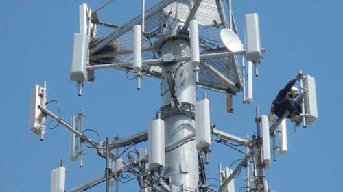
The first stepping stone towards 4G is LTE (which stands for Long Term Evolution if you must know, not that that really helps). It comes in 5 categories of which the most common are 3 and 4 offering a downlink speed of 100 or 150 Mb/s and an uplink speed of 50 Mb/s. Tensilica already has products in this space that they have been shipping for quite some time, both for handset applications and also for basestations (of all flavors: macro, picocell, femtocell). Network buildout for LTE has been taking place over the last year or so and phones using this technology are just starting to come to market (no, iPhone 4S does not support LTE but the iPad 3 is rumored to be going to). Buildout will continue for another year or two, with 1.5 million LTE basestations expected to be installed by 2015 (In-Stat). NEC, Fujitsu, Panasonic, Huawei and others are making use of Tensilica’s earlier ConnX DSP family for LTE implementation.

True 4G is known as LTE-Advanced, categories 6 and 7 (everyone seems to be skipping category 5) with downlink speeds of 300 Mb/s and uplink speeds of either 50 or 150 Mb/s. The performance increase required is 2-5X that required for LTE, but since we’d like our phones to continue have good battery life, the power budget is pretty much the same: 200 mW. The challenge is how to design such a modem with much higher performance and no increase in power. The two extreme approaches, that have often been used in the past, are either to design RTL and create a special hardware block, or else use a general purpose digital signal processor (DSP). The first approach is expensive and inflexible, and the DSP approach consumes too much power. One major handset OEM who has taken the RTL approach up until now says “we can’t do that any more for LTE-A”.

What Tensilica is announcing today is the BBE32UE (catchy name huh?). This is, of course, built on top of Tensilica’s Xtensa technology. It is a specialized LTE-Advanced processor that can be programmed in C. The processor itself dissipates about 45 mW. It is a SIMD 3 issue VLIW processor that works with Tensilica’s almost optimal scheduling and optimization C-compiler (which apparently now has over 100 man years of effort in it).

Along with some other specialized processors (or IP blocks) for FFT and FIR a fully-programmable LTE-A category 7 modem can be built that meets the 200 mW power budget (in a 40nm low-power process). Early access customers have the product now but general release will not be until Q3.

More details on Tensilica’s digital signal processors for LTE and LTA-Advanced are here.


Pinpoint: Getting Control of Design Data

Pinpoint: Getting Control of Design Data
by Paul McLellan on 02-20-2012 at 5:39 pm

Back in the Napoleonic era it was possible to manage a battle with very ad hoc methods. Sit on a horse on top of the highest hill and watch the battle unfold, send messengers out with instructions. By the First World War, never mind the second, that approach was hopelessly outdated and a much more structured way of managing a battle was required. Chip design is a bit like that. Until recently, people could manage a design using ad hoc methods like Excel but now the Napoleonic era is over and a much more structured and disciplined approach is required. Otherwise all designs are like the famous aphorism: it takes 90% of the time to do the first 90% of the design, and the other 90% of the time to do the last 10%.

You see this all the time. Everyday, chip tapeouts slip their schedule and managers wonder why they didn’t see the issues sooner. Engineers grapple with communicating and resolving issues and even understanding the real status themselves. Closure is always a few days away, “real soon now.”

Many companies realize that this is an issue and have invested a few people in building some sort of system to allow them to keep track of where their design is. But it turns out that doing this on the cheap without a good underlying infrastructure is harder and more expensive than it looks.

One company I’m on the board of (actually the only one) is Tuscany Design Automation and they have created a product, Pinpoint to address this problem. It focuses on providing teams with hard information that they need to get the design closed and taped-out sooner. It generates actionable information to engineers and managers by extracting critical metrics from existing tools at each step of the flow. It is “design literate” able to read physical design, netlist and timing files directly rather than trying to naively parse reports. Everything is based around a central project server accessed through a browser, enabling collaboration and communication among team members.

Improving overall team performance without adding team members (and so money) is one of the best actions that a manager can make. And a good way to do that is to eliminate existing inadequate mechanisms for communication (such as everyone extracting design data and manually adding it to a wiki). Some companies find they have several hours of meetings every day to try and get to grips with where things stand and update assignments. In such an environment the team efficiency goes way down. Pinpoint directly goes into the data and makes the issues visible. It even provides functionality for status reporting using objective data and not subjective “95% done” updates.

As Ralph Portillo of Netlogic (now part of Broadcom) said: “I don’t want to say I can’t live without Pinpoint but I can’t live without Pinpoint.”

The Pinpoint information page is here.


PLL Design Challenges for Integrated Circuit Designs

PLL Design Challenges for Integrated Circuit Designs
by Daniel Payne on 02-20-2012 at 10:54 am

Nandu Bhagwan is CEO of GHz Circuits and has been designing PLL circuits used in ICs for the past 12 years. Mr. Bhagwan did a video interview with John Pierce of Cadence to talk about the challenges of PLL design.
Continue reading “PLL Design Challenges for Integrated Circuit Designs”


Semiconductor IP Becomes A Critical Element in ASIC Design

Semiconductor IP Becomes A Critical Element in ASIC Design
by Daniel Nenni on 02-19-2012 at 4:05 pm

Clearly one of the market trends proving troublesome in the traditional ASIC value chain is the lack of silicon correlated custom IP. And make no mistake, semiconductor IP is a critical decision since it drives both chip level and system level technology differentiation.

Under the traditional ASIC model, vendors had their own IP, silicon-proven and tuned to their own fabs. This was a good thing as it assured a fast ramp to volume and more predictable yield curves. The downside was that IP catalogs were somewhat limited which constrained product differentiation. And now a staggering 49 fabs were shut down in 2009-11 as traditional ASIC vendors and IDMs continue to go fabless.

Fortunately there is a new value chain model in play today that provides all of the silicon-proven IP benefits of the classic ASIC value chain model and provides a broader portfolio of in house-developed and third party IP. As a long time IP guy I can tell you that this is of great importance! The semiconductor ecosystem revolves around IP, it is the lifeblood of our industry!

The new model, now being promoted by Global Unichip Corporation (GUC), is called the Flexible ASIC Model[SUP]TM[/SUP]. It’s built on the premise that a company should not be constrained by its own assets such as manufacturing, IP, test or assembly, but rather should be able to focus on providing the most efficient design and the fastest time-to-market. This is a critical component that makes the Flexible ASIC Model work.

Make no mistake, while GUC provides streamlined and robust integration of third-party IP, it has not overlooked, and has in fact invested heavily in, its own IP development capability. As I blogged in Semiconductor IP Dilemma, four years ago GUC was an IP baron design services provider. Now GUC has a full lP portfolio with custom IP design groups in Taiwan, China, and Silicon Valley.
Much of GUC’s in-house developed IP covers SerDes, Data Converters and DDRs. The rationale for developing these particular blocks in-house is that these are the micros with the greatest demand and differentiation for the SoC ASIC marketplace, and I agree completely.

The main advantages of using in-house developed IP is the ability to know the precise effects of packaging and boards on the signal because the company has end-to-end supply chain capabilities and often end-to-end responsibilities.

By integrating IP development and implementation with package design, board design, and chip design, a Flexible ASIC Provider can simulate the complete system performance before sending the device to the manufacturing. The real key in this whole process is the capability to test for board effects and signal integrity then to be able to predict those impacts on the system and on the IP.

The secret to achieving superior performance, low power, and area balance lies in the hybrid analog/digital IP architecture that GUC uses to design its IP. This plus the access to advanced technology nodes, thanks to its very close working relationship with manufacturing partner TSMC, creates key differences that have proved critical to ASIC developers. Remember, GUC is directly across the street from TSMC Fab 12.

IP availability is absolutely becoming a critical differentiation and a much discussed option in the design community. Which raises the question of the day:

What are some of the hardest to find critical IP that you need to fit your current and future designs?


Semiconductors: A Decade of Invention… A World of Solutions

Semiconductors: A Decade of Invention… A World of Solutions
by Daniel Nenni on 02-17-2012 at 1:53 pm

Please join IBM, Samsung Electronics, Co., Ltd., and GLOBALFOUNDRIES at the 2012 Common Platform Technology Forum. The forum will showcase the alliance’s technological progress and how joint collaboration and innovation is setting the direction for industry-leading solutions to enable next-generation products.

Continue reading “Semiconductors: A Decade of Invention… A World of Solutions”


Multicore SoC Architecture Optimization

Multicore SoC Architecture Optimization
by Eric Esteve on 02-16-2012 at 5:36 am

Once again with Synopsys and Arteris, the innovation is coming to solve an issue, faced by their potential customers: “In our research, we’ve found that almost half of project delays are caused by problems with the system architecture design and specification,” said Chris Rommel, vice president, embedded software and hardware, VDC Research. “Many of these architecture problems are related to escalating SoC complexity, including multicore requirements. Therefore, solutions like the one developed by Synopsys and Arteris to efficiently analyze multicore SoC architectures early in the design flow should become increasingly valuable as engineering teams look for ways to help improve project schedules and performance results.”

From a pure business point of view, Arteris and Synopsys teaming up to solve problems related to SoC complexity, including (ARM based ?) multicore requirements makes a lot of sense: both ARM and Synopsys have invested into Arteris, along with Qualcomm, the others being VC. When building a partnership, this is a very good sign of success when the two companies also have common business goals! And that’s good for the future customers, as they know that they will invest money, and also large engineering resources, into a solution which has a real future – which is not only a good way to make market communication! You can see the PR here.

Let’s have a look at what is behind this communication. The SoC development platform from Synopsys, Platform Architect environment with Multicore Optimization Technology (MCO), has been enhanced with transactors and analysis monitor support for Arteris’ FlexNoC interconnect models. The new MCO offers system architects three distinct advantages for early performance analysis and optimization of complex designs:
1.obtaining fully-instrumented performance models before software and RTL availability,
2.clearly measuring and visualizing the dynamic behavior and performance bottlenecks of multicore designs, and
3.automating the design flow to enable developers to explore hundreds of architecture alternatives in days versus weeks or months with paper specifications and RTL methods

The benefit of this faster turnaround time is that architects using FlexNoC interconnect IP can more fully explore and optimize their multicore architectures and then avoid to over- or under-design their SoC. Both can have a dramatic cost impact: if you over-design the SoC, you will spend endless time to complete the design and release it to production, loosing precious Time-To-Market, which can easily turn into much more money than the already large SoC development cost. If you under-design the SoC, you will probably hit the market window, but with a product comparing poorly with the competition, then lose market share.

“Our goal is to help system designers and architects avoid late discovery of system performance problems that can be extremely costly for both project schedules and budgets,” said John Koeter, vice president of marketing for IP and systems at Synopsys. “By starting architecture analysis and optimization at the transaction-level with Arteris’ FlexNoC interconnect models in Synopsys’ Platform Architect MCO, we offer SoC architects the ability to perform accurate simulation of the multicore system and its most critical application use-cases earlier. With this combination they can achieve the best balance of performance, power and cost at a time in the development process where they have the greatest impact.”

“Arteris FlexNoC’s integration with Synopsys’ Platform Architect MCO environment allows our customers to create better SoCs in less time,” said K. Charles Janac, president and CEO of Arteris. “Integration of the two technologies allows SoC designers to have the same quick turn-around simulation times they experience today with FlexNoC, while gaining critical benefits from the more realistic simulation and earlier analysis of their application scenarios.”

I have blogged in previous post about Arteris FlexNoC’s silicon-proven commercial network-on-chip interconnect IP offering the ability to reduce the number of interconnect wires and logic required for multicore SoC design. Reducing the interconnect wires and logic gates resolves routing congestion and timing closure issues at the back-end place-and-route stage, resulting in shorter development cycle time, faster SoC frequencies, smaller SoC area and less SoC power.

I have also blogged about Sonics vs Arterislegal battle(s), but I honestly prefer to discuss about such a partnership, as it clearly demonstrate who is bringing real innovation on this IP market!

Availability
Arteris and Synopsys’ integration is available today for users of Arteris FlexNoC version 2.6 or later, and Synopsys’ Platform Architect MCO tool version G-2011.06-SP2 or later. For more information on Arteris’ FlexNoC interconnect IP, please visit: www.arteris.com/flexnoc. For information on Synopsys’ Platform Architect MCO tool environment, please visit: http://www.synopsys.com/platformarchitect.

By Eric Estevefrom IPNEST