RVN! 26 Banner revised (800 x 100 px) (600 x 100 px)

Farm Management

Farm Management
by Paul McLellan on 03-01-2012 at 5:34 pm

Every so often I come across a new company in EDA or one of its neighboring domains, new to me anyway, and new to SemiWiki. One such company is RunTime Design Automation (RTDA). They provide a suite of tools for managing server farms (or internal clouds which seems to be the trendy buzzword du jour). Running a few EDA scripts on a few servers is something that is not too hard to do, but when you are looking at running tens of thousands of jobs on thousands of servers, you have a whole new set of problems. Servers crash or hang. Tools run out of licenses. Jobs depend on each other in a complicated tree. These are the problems that RTDA addresses.

When I was at Ambit we had a Q/A farm of 40 Sun workstations and 20 HP workstations, an unusually large investment at the time. Now this is a trivially small farm in an era when data-centers may house 100,000 servers and literally millions of jobs a day need to be scheduled.

RTDA have four products:

  • LicenseMonitor
  • NetworkComputer
  • FlowTracer
  • WorkloadAnalyzer


The simplest product is LicenseMonitor. It pulls license usage data from the license servers used by EDA (and other) tools, such as FLEXlm. This gives a summary of what license usage really is so that a company does not end up either having too few licenses and thus wasting time when running jobs, or having too many licenses and wasting money. It also interfaces with Network Computer to ensure jobs are not scheduled until licenses are available.


NetworkComputer is the highest performance job scheduler to spread a workload over a large server farm. It is similar to the well-known LSF but more powerful and better integrated with EDA license management. It has a GUI that allows a user to keep track of thousands of jobs, which are color coded as they become runnable, start to run, crash, complete and so forth. It can handle millions of jobs on thousands of processors. It can get license usage of, for example, simulation licenses up to very close to 100%.


FlowTracer is a much more sophisticated tool like the Unix make command that manages complex design flows, handing all the dependencies, errors and so on. It handles the entire design flow giving visibility to what is happening and automatically updating dependencies intelligently.

Finally, WorkloadAnalyzer is a server farm simulation allowing efficient compute farm planning, answering questions such as what would happen if additional servers or additional licenses were purchased. It can be used daily for planning or annually to provide data for license renegotiation. It can take information from Network Computer (or its competitors) and analyze how that workload would run under different circumstances and thus make it easier to optimize the investment.

Download the free e-book, The Art of Flows here


3D Transistor for the Common Man!

3D Transistor for the Common Man!
by Daniel Nenni on 03-01-2012 at 3:28 pm

The 1999 IDM paper Sub 50-nm FinFET: PMOSstarted the 3D transistor ball rolling, then in May of 2011 Intel announceda production version of a 3D transistor (TriGate) technology at 22nm. Intel is the leader in semiconductor process technologies so you can be sure that others will follow. Intel has a nice “History of the Transistor” backgrounder in case you are interested. Probably the most comprehensive article on the subject was just published by IEEE Spectrum “Transistor Wars: Rival architectures face off in a bid to keep Moore’s Law alive”. This is a must read for all of us semiconductor transistor laymen.

My first pick of talks at this month’s Common Platform Technology Forumwill be given by Dr. Greg Yeric, ARM Consultant Design Engineer, R&D. Greg has 20 years of semiconductor experience beginning with Motorola/Freescale, HPL, which brought him to Synopsys through acquisition, and for the last 4+ years he has been at ARM. Greg’s talk “IP Design and the FinFET Transition”will cover foundry access to finFETs. Here is a reprint of an interview with Greg from the Tech Design Forum Newsletter in case you have not seen it:

TDF: What is the big deal about finFETs and what do they mean for IP?

FinFETs hold the promise of being fundamentally better switches than bulk planar transistors. So, they’ll allow favorable power and performance scaling beyond 20nm. However, they are a new kind of transistor with new issues and limitations. They are different enough that one runs the risk of producing sub-optimum IP without good understanding and planning. But properly executed, they’ll mean that 14nm delivers better power and performance.

How big a change are finFETs?

On one hand, they have the same metal-oxide-semiconductor structure, simply folded up, accordion-style, to provide a higher current density. In that sense, designers will see them behave in familiar ways. The key change will be a sizeable bump in the roadmap for some scaling parameters. There’ll be enough notable differences that the transition should offer an opportunity to assess the scaling of our designs.

What specifically should designers be aware of?

Most everyone has heard about quantization – that the finFET drive strength is varied by the number of discrete fins in parallel. For that reason and others, low power designers will face a different granularity in choices than they’ve been used to. Another potentially more interesting side-effect of quantization is a new fin-metal gear ratio. Designers must plan for the fact that finFETs offer a change in the scaling compared to recent nodes. Delay and power can be improved in aggregate, but their components, represented by CV/I and CV^2f, will scale in different ways. I wouldn’t recommend a lazy extrapolation of past trends.

What other differences might there be?

The variability signature will probably change. finFETs improve some aspects of variability but because they have new process components, I’d expect to see other new variation issues. This shift might foretell a change in the balance between local and global variation that will affect memory and logic differently. Also, scaling to 14nm in and of itself won’t be easy, and all of the finFET issues will have to be folded – no pun intended – into this broader context. I’ll discuss a broader process scaling perspective at the forum.

My big question is parasitic extraction of 3D Transistors, how is that going to work?


2012 semiconductor market could decline by 1% or more

2012 semiconductor market could decline by 1% or more
by Bill Jewell on 02-29-2012 at 6:00 pm

The world semiconductor market grew a slight 0.4% in 2011, according to WSTS. In early 2011, expectations were for growth in the 6% to 10% range. Various natural and man-made disasters lead to weaker than expected growth. The March 2011 earthquake and tsunami in Japan disrupted semiconductor and electronics production. Floods in Thailand in 3Q and 4Q 2011 severely impacted hard disk drive manufacturing. The European financial crisis resulted in weak demand in 4Q 2011.
Recent forecasts for the 2012 semiconductor market are primarily in the range of 2% to 3%. Always optimistic Future Horizons predicted 8% growth. IC Insights projected 7% growth for the IC market. We at Semiconductor Intelligence believe the 2012 semiconductor market will see a slight decline of about 1%. The decline is expected due to the overall economic outlook in 2012 and the quarterly pattern of the semiconductor market. (Cick to enlarge images)

The International Monetary Fund’s (IMF) January 2012 forecast was for World GDP growth of 3.3% in 2012, half a point slower than estimated 3.8% growth in 2011. The U.S. is expected to maintain moderate 1.8% growth in 2012, the same as in 2011. The Euro Area is projected to see a 0.5% drop in GDP in 2011 due to the financial crisis. Japan’s GDP should rebound from a 0.9% decline in 2011 to 1.7% growth in 2012 as it recovers and rebuilds from the 2011 disasters. China remains a major growth driver, with expected 8.2% growth in 2012, one point lower than in 2011. Hong Kong, South Korea, Singapore and Taiwan collectively should see 3.3% growth in 2012, slowing from 4.2% in 2011.

The semiconductor market declined 7.7% in 4Q 2011 from 3Q 2011, due largely to the floods in Thailand and weakness in Europe. The largest semiconductor companies providing guidance generally expect significant revenue declines in 1Q 2012 from 4Q 2011. Intel, Texas Instruments, ST Microelectronics and AMD all gave similar revenue guidance: worst case declines of 10% to 12%, best case declines of 4% to 5%, and midpoint declines of 7% to 8%. Renesas and Broadcom also expect declines in 1Q 2012. Samsung did not give specific guidance, but expects a weak DRAM market in 1Q 2012. A couple of companies expect increases. Toshiba expects a recovery to 15.5% revenue growth for its semiconductor business after a 19% decline in 4Q 2011. The midpoint of Qualcomm’s guidance is for 2.5% growth.

We at Semiconductor Intelligence are forecasting a 5% decline in the semiconductor market in 1Q 2012. With a 5% 1Q 2012 decline following the 7.7% decline in 4Q 2011, it will be difficult for the industry to achieve positive growth for the year 2012. The average quarter-to-quarter growth rate in 2Q through 4Q 2012 would need to be 6.5% just to achieve 0% for the year. Our forecast of a 1% decline in 2012 is based on average growth of about 5% for the last three quarters. Further deterioration in the world economic situation from current expectations could result in a more significant decline in the semiconductor market in 2012 of 5% or more.


Synopsys MIPI M-PHY in 28nm introduction with Arteris

Synopsys MIPI M-PHY in 28nm introduction with Arteris
by Eric Esteve on 02-29-2012 at 8:05 am

MIPI set of specifications (supported by dedicated controllers) are completed by a PHY function, the D-PHY or the M-PHY function. The D-PHY was the first to be released, and most of the MIPI functions supported in a smartphone we are using today probably still use a D-PHY, but the latest MIPI specifications have been developed based on the M-PHY usage. Which does not means that the D-PHY will disappear any soon, but clearly M-PHY is the future…

At the early days of MIPI introduction, Synopsys was not as comfortable with MIPI as an IP product, as you could not consider the M-PHY as a “one size fits all” traditional IP product: the specification defines M-PHY Type I, Type II, and within these Type, another set of options, High Speed Gear 1, 2 and 3 for Type II and for type I the same, plus Pulse Width Modulator (PWM) 0, 1 to 7. This way to define one product, but with multiple options to be supported, was hurting Synopsys product marketing approach, which is to develop one product, and address a market as wide as possible using a large sales force… this is in fact the definition of an IP business!

The discussion I had last week with Navraj Nandra, Marketing Director for Mixed-Signal IP (including the PHY Interfaces product line), shows that Synopsys has found a way to solve this business issue with an elegant engineering solution: the MIPI M-PHY developed by Synopsys in 28nm is a modular product. If a customer needs to implement the M-PHY Type II supporting Gear 1 to 3, he will integrates this function only. This is the best way to optimize the associated footprint and power consumption, and it is easier than to follow the other potential route which was to engage an IP or design service company to specifically develop the function supporting the part of M-PHY specification to be supported.

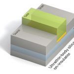
Because at Semiwiki we try to do some evangelization, let’s see what are the functional (specific) specifications associated with the M-PHY (agnostic by nature). I strongly engage you to have a look at the above picture!

At first, let’s start with the “pure” MIPI specifications, in that sense that these have been developed by the MIPI Alliance alone:

  • DigRF v4 is the specification allowing to interface with RF chip (supporting LTE), can be connected directly to the M-PHY.
  • Low Latency Interface (LLI) can also be connected directly to the M-PHY. We will come back later in this paper to LLI, as the release 1.0 has been announced this week, at MWC
  • CSI-3, the Camera Interface, has to be connected through UniPro, an “agnostic” controller, to the M-PHY
  • DSI-2, the Display Interface, connect to the M-PHY also through UniPro
  • Universal Flash Storage (UFS), a specification jointly developed by JEDECand MIPI, to support external Flash devices (Card), also connect through UniPro
  • Finally, another specification has been jointly developed, with USB-IF, called SuperSpeedIC (SSIC), allowing to connect two USB 3.0 compatible devices, directly on a board (no USB cable)

To summarize, M-PHY and UniPro are agnostic technical specifications (one mixed-signal, the other digital), and CSI-3, DSI-2, DigRF v4, LLI, SSIC and UFS are function specific specifications, defined by MIPI Alliance alone, or by MIPi Alliance and USB-IF, or JEDEC for respectively the last two.

MIPI has the potential, from a technical standpoint, thanks to the benfits it brings in term of High Speed Serial AND low power Interface, and in term of interoperability, to be used in PC, Media Tablet and Consumer Electronic segments, on top of the Wireless handset segment. MIPI Alliance has the willingness to support such a pervasion, but doing some evangelizationwill be necessary for the MIPI specifications to go to the mainstream, Consumer electronic or OC segments!

LLI Specification has been officially released by the MIPI Alliance, at the occasion of the Mobile World Congress in Barcelona, this week. As indicated by the name, the round-trip latency of the LLI inter-chip connection is fast enough for a mobile phone modem to share an application processor’s memory while maintaining enough read throughput and low latency for cache refills. Sharing the same DRAM device means the wireless handset integrator can save real estate printed circuit board (PCB) space and create a thinner smartphone, or implement additional device, more features to the smartphone, like NFC chip for example. It also means that the OEM will save, on every manufactured smartphone, the cost of one DRAM ($1 to 2$). If you manufacture dozen of million smartphone like some of the leaders, you can see how quickly you will get the return on the initial investment done by the chip makers to acquire the IP!

MIPI Alliance is strongly supportive of LLI, as we can see from this quote: “As active MIPI contributors, Synopsys and Arteris are aiding in the adoption of the MIPI M-PHY and MIPI Low Latency Interface,” said Joel Huloux, chairman of the board of MIPI Alliance. “The early integration and availability of the Arteris and Synopsys solution helps speed time to market for MIPI LLI adopters.” LLI support from Arteris and Synopsys illustrate how important is to build a strong partnership when selling a complementary solution, as the joint solution consists of Arteris’ Flex LLI™ MIPI LLI digital controller IP and Synopsys’ DesignWare® MIPI M-PHY IP. A team of Arteris and Synopsys engineers, formed to facilitate verification and testing of the joint solution, validated its functionality and interoperability.

And for those who love to get insights, you should know that LLI was initially developed by an Application Processor chip maker, who understood that the function, to be successful on the market, has to be marketed and sold by an IP vendor, Arteris was selected as they were already marketing C2C or “Chip To Chip Link” IP, offering exactly the same functionality (sharing a DRAM between Modem and Application Processor), by the means of a parallel Interface in this case, but we will come back soon about this IP.

Eric Esteve – See “MIPI IP Survey & Forecast” from IPNEST


Huawei and Intel Redrawing the New Mobile Playing Field

Huawei and Intel Redrawing the New Mobile Playing Field
by Ed McKernan on 02-28-2012 at 7:22 pm

This time is differentis a book that was released just months before the financial crises in 2008 describing hundreds of historical cases where smart people ended up making disastrous decisions over the span of 800 years that led to government defaults, banking panics etc… In the semiconductor industry, we also tend to think this time is different due to the rapid advancements made possible by Moore’s Law. A year ago the ARM camp (nVidia, TI, Marvell, BRCM) was riding high at the prospects of winning the mobile market and casting Intel aside. Now, I would argue, that Apple’s stunning growth has forced a completely new game on the industry. In this game the phone carriers are in desperate need for an alternative and Intel and Huawei, with their announcements this week, have shown the way to “save the carriers.”

You want to talk about big money, AT&T’s revenue was $127B in 2011 and Verizon’s was $111B. Repeat these numbers with the carriers the world over and it becomes obvious that there exist a big leagues (call it the $100B club), that few suppliers can play in. Apple frightens the carriers because they have to shell out all the Cap Ex to handle the mobile tsunami imposed by Apple’s iPhone and iPADs. Starting with the 4G LTE enabled iPAD 3 in March and followed by a similarly enabled iPhone 5 in the fall, the tsunami data waves will increase in a magnitude that will be more than a step function. What shall they charge customers for the data onrush, no mathematician can foretell. However, whatever it ends up being, one thing is sure: Apple will have a hand in negotiating the business model.

Five years ago Nokia could never have imagined getting away with selling a phone to carriers for an average of $660. With the iPAD 3 with LTE, expect it to go higher. Apple’s roughly 60% gross margin is significantly more than what they receive for the MAC PCs and is a sense causing the carriers to see a future bloodbath. The carriers need an alternative house brand that provides margin relief and counterweight to Apple, who will likely ramp up to at least 50% of their customers. So while they can not live without Apple, they can’t survive on them alone.

Which brings us to this week and the announcement that Huawei is building its own quad core processor for smartphones and that Intel has made agreements with the UK carrier Orange, the Indian carrier Lava and Chinese equipment manufacturer ZTE to build and sell Medfield based smartphones this year. It should be noted that Huawei and ZTE are the #1 and #2 Chinese Telecom and Networking equipment vendors and furthermore they are both in the top 5 in mobile handsets.

The announcement of Huawei building their own processor is another sign that independent silicon suppliers like nVidia, TI, Marvell and Broadcom will see less fertile grounds to plow in the mobile space. In the last earnings call, nVidia CEO Jen Hsun Huang admitted that sales of Tegra 3 would come in much lower than expected for 2012 because Samsung had decided to use their own in house processors. Vertical integration is the trend and it is absolutely necessary.

Looking much further down the road though, Huawei and Intel appear to be on similar tracks with a slight twist. Huawei is going to go completely in house vertical with the smart phones and telecom equipment with some assist from Qualcomm on the 4G LTE in phones and base stations. They will offer a package deal to carriers – buy the telecom and networking equipment and get the phones at a discount. The net is an increase in cash flow to carrier over buying phones from HTC or Samsung and equipment from Huawei, ZTE, Cisco or Ericsson.

ZTE looks like it will rely on Intel for silicon not only for cell phones but I am guessing also for networking and future telecom gear. Huawei is financially more powerful than ZTE and has in fact set up a design center in Silicon Valley staffed with ex-Cisco engineers to build high end ASICs for Routers and Switches. Their footprint is growing.

With what they believe is a 4 year lead in process technology, Intel is now going to execute a strategy of offering what will be lower cost, lower power silicon in the smartphone and tablet space by the time they convert Atom to 22nm in early 2013. On the other side of the house, it appears that they will expand their data center offerings to the point they can deliver the silicon a ZTE needs to be competitive with Huawei. All of this will likely have an “Intel Inside” marketing pull through the carriers.

As mentioned in a previous blog, the era of independent Fabless chip companies who rely on the leading edge is coming to an end. The winners will own Fabs (ie Intel or Samsung), have IP or be vertically integrated like Apple or Huawei who bury the processor in the total BOM of the phone. Both though will be tempted to jump to Intel to gain access to the latest process technology and gain an edge on Samsung.

For the carriers, they see a need to immediately address the bottom line before Cap Ex overwhelms them. For Huawei, ZTE and Intel the doors of opportunity have just opened up. More Importantly, for Intel this time is no different than how they executed in the 1990s PC Market.

Now, with regards to Google….

FULL DISCLOSURE: I am long AAPL, INTC, ALTR, QCOM


HSPICE Users Talking about Their Circuit Simulation Experience

HSPICE Users Talking about Their Circuit Simulation Experience
by Daniel Payne on 02-28-2012 at 4:46 pm

tony todesco

HSPICE users gathered in January 2012 at the HSPICE SIG(Special Interest Group) to talk about their experiences using this circuit simulator for a variety of IC and signal integrity issues. I wasn’t able to attend in person however I did watch the video and wanted to summarize what I heard:
Continue reading “HSPICE Users Talking about Their Circuit Simulation Experience”


Does 14nm magically put Intel back on the lead smartphone lap?

Does 14nm magically put Intel back on the lead smartphone lap?
by Don Dingee on 02-27-2012 at 2:15 pm

I’ve often wanted to publish a book with nothing but photos of police cars, so that people wouldn’t have to slow down and gawk at them when they have someone pulled over on the side of the freeway. Intel roadmaps seem to have the same effect on people. No matter what is on them, even if there’s nothing really new, they stop people in their tracks just to look.

At Mobile World Congress today, Intel’s Paul Otellini created the latest traffic jam by laying out the plans to move from the Atom Z2460 (Medfield) at 32nm into the Atom Z2580, targeting their new 14nm process in two years. Also, he previewed the Z2000, the first “value” tier push targeting lower cost implementations.

Intel firmly believes they can compete in mobile, and is betting the farm on 14nm to catch up. With roughly twice as many transistors to deal with compared to an ARM Cortex-A9 core, they’re looking to faster memory interfaces, FinFETs, and process shrinks to get it done.

The push to 14nm isn’t surprising at all: Intel has to fill Fab 42. It’s the only play. With the news of HP shrinking their way to greatness in the PC business, it will have to come from Atom, smartphones, and embedded … er, intelligent systems.

While the initial Atom Z2460 performance numbers are in the range of the Qualcomm MSM8960 (BrowserMark: 116425 vs. 110345), they are coming at substantially higher power consumption – about 1W versus something less than 750mW, maybe as low as 450mW. The performance/watt figures still favor the ARM camp, by a lot, and that ecosystem isn’t standing still with things like the Cortex-A7 coming.

Intel has a huge gap to close here, and it’s good to see they are competing to get back on the lead lap, but they have a lot of work left to do.


Yalta is Dead! Synopsys offensive in VIP restart the cold war

Yalta is Dead! Synopsys offensive in VIP restart the cold war
by Eric Esteve on 02-27-2012 at 11:29 am

Last year, you could claim (like I did in this blog) that Cadence was making money with large VIP port-folio, when Synopsys was managing sales of a large Design IP port-folio (thanks to a successful acquisition strategy in the 2000’s). But the latest acquisitions made by Synopsys of VIP centric companies like nSys or ExpertIO should have warned us (and Cadence, by the way): the EDA and IP centric company is investing the VIP field! After the acquisitions time come the new product launch, today the market is discovering… Discovery.

It looks like this product launch is a real offensive, and much more than just an announcement. Synopsys Discovery VIP is written entirely in SystemVerilog, includes native support for UVM, VMM, and OVM, and is compatible with all related verification environments… and supports all major simulators, including Cadence Incisive (!), the product realizes a breakthrough in the VIP jungle. Because of the multiple competing above mentioned standards (UVM, VMM and OVM), the only way to support all of these (and it was a strong market requirement) for a VIP product was to use wrappers. By using wrappers, on top of making the product inelegant, you made it slower. Diminishing simulation run time, offering a performance improved by 3 to 6X is a strong sales argument, I am sure that Synopsys’ sales force will be the first to benefit from this argument, the second being the customers!

Such an argument is based on an identified issue, that every design team trying to complete a SoC design, every marketing team fighting with Time To Market issue, every shareholder expecting a high return on investment knows very well; the cost and elapsed time due to Verification. In fact, I am not so sure that the basic shareholder understands anything about Verification, but he should understand ROI! The next picture is useful to understand the cost breakdown associated with Verification. If you look at the middle left box, you see a 3X cost (or license count, or resources) increase for almost every task (except “Tool, Support and Service” with 20% only, so I suspect that Synopsys will sell Discovery 20% higher than the previous solution?). So, offering a 3 to 6X run time improvement is welcome, to keep the design schedule and consequently the time to market within reasonable limits.

If you look at the product itself, Synopsys includes with Discovery VIP, a Protocol Analyzer which enables engineers to quickly understand, identify and debug protocols in their designs, and debug and coverage management features, so the complete solution is built within a single product.

If we look to Synopsys VIP port-folio, we can see that the war with Cadence will be face to face, protocol by protocol, as they both address the same customer needs. Except for the Memory Models, that Cadence is marketing after Denali acquisition, and where Denali had a monopoly for a long time, but on what constitute the Verification IP market, still to be evaluated, but probably in the $100 to $150 million range, we can expect to see an interesting battle. I am just waiting to know what will be Cadence’ answer to Synopsys’ Discovery offensive!

From Eric Estevefrom IPnest


ISSCC 2012: Silicon Systems for Sustainability!

ISSCC 2012: Silicon Systems for Sustainability!
by Daniel Nenni on 02-26-2012 at 4:00 pm


What can we do for Earth’s sustainability? Besides sorting our garbage and recycling our lawn clippings? Sustainability must be the paramount theme for the future of human society! Semiconductors for a better life! Well, according to my kids, if you take away their smart phones there is no life!
Continue reading “ISSCC 2012: Silicon Systems for Sustainability!”