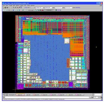
 One of the challenges with today’s SoCs is that chip-finishing, putting the final touches to the SoC working at the chip level, stresses layout editors to the limit. Either they run out of capacity to load the entire chip, or they can handle the entire chip but everything is like wading through molasses, it takes an awfully long time to get anything done.
As a result there are a number of chip viewer tools that focus just on being able to load the SoC and very fast to display. The problem with these is that editing capabilities are either non-existent, it is strictly a viewer, or extremely limited.
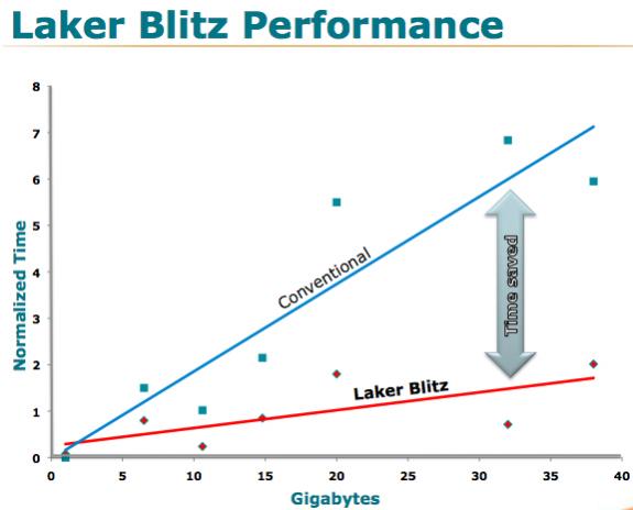
 Laker’s Blitz is a tool that brings the best of both worlds. It can handle extremely large designs and is between 5 and 20 times faster than regular layout editors. However, it has most of the editing features that regular layout editors have since it is built on top of Laker Custom Layout. It has the same user-interface, same basic editing, same in-memory schema, same integration with DRC/LVS, and the same Tcl extensions.
Blitz is optimized for chip-level operations on very large chips, basically reading GDS, editing, and then writing the GDS back out again. The four big tasks it has been optimized for are:
- Chip-finishing: chip-level review, editing, assembly and debugging
- IP merging: replacing IP black-boxes with physical layout
- SoC assembly and review: assemble IP blocks, trace critical nets, verify and fix boundary DRC errors
- DRC review and repair: chip-level signoff DRC
Of course not every single thing that you can do in Laker Custom Layout is supported, otherwise it would make no sense to have two tools. In particular, Laker Blitz is 64-bit only, it cannot create or modify Pcells and so on. It is focused strictly on the typical tasks done at the chip level with today’s advanced technology node SoCs.


Is Intel About to Take Flight?