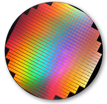
 One of the most demanding areas of layout design has always been memories. Whereas digital design often uses somewhat simplified design rules, memories have to be designed pushing every rule to the limit. Obviously even a tiny improvement in the size of a bit cell multiplies up into significant area savings when there are billions of memory cells on a chip. It’s like that 9/10c per gallon at the gas station. It’s just a dime or so to you, but for Exxon it is real money.
Starting from its home base in Taiwan, Laker has been successful at capturing many of the big names in memory design in Asia. Hynix (based in Korea of course), Winbond and Eon (a newly public fabless memory company based in Taiwan) are all customers. Between them they cover DRAM, NAND flash, NOR flash and lots of specialized memory products for graphics and mobile.
But once you get outside the core itself, memory is no longer designed completely by hand, the automation from custom digital routing (driven off the desired connectivity) is an important part of productivity. To be useful in this sort of demanding layout environment it needs to be both gridded and shape-based, tuned for memory-specific routing styles such as main and secondary spine routing and limited routing layers (remember, memories like to keep metal cheap).
So memory layout is one of the most demanding application spaces of all. When I was at VLSI Technology our corporate counsel came from Micron and was amazed at the difference: “we put a design into production about once a year, here you do it about once a day.” Well, the memory market is no longer like that. It may not have quite the churn of new designs that a full-blown ASIC business does, but it is moving in that direction.
More information about Laker’s custom digital router here
Share this post via:


Musk’s Orbital Compute Vision: TERAFAB and the End of the Terrestrial Data Center