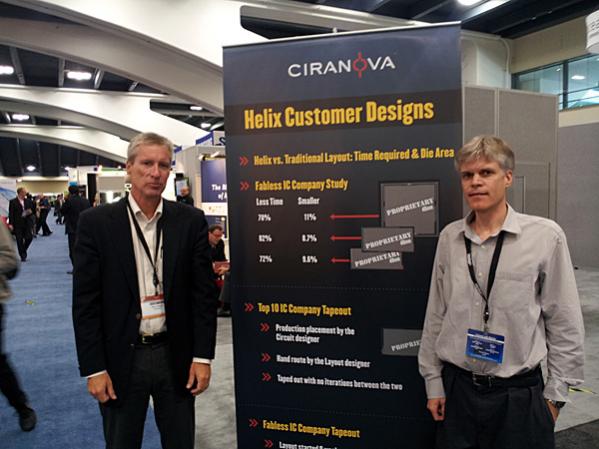
Three people from Ciranova met with me at DAC this year: Eric Filseth (CEO), David Millman (Marketing) and Lindor Hendrickson (CTO). They gave me an update on how the Helix tools are being used to automate the layout of custom IC designs at 28nm and smaller nodes.

Eric Filseth and Lindor Hendrickson
Our PyCells™ are interoperable, DRC-correct, and use state-of-the-art object-oriented software technology to dramatically reduce the effort needed to create and maintain PCells, especially at 65nm and below. PDK groups creating PyCells build design kits with much less effort, and respond radically faster to their circuit designer customers, than do traditional PCell users.
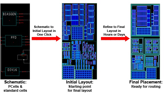
Our Helix™ device-level placement software slashes physical design time, lets design teams optimize their floorplans for performance and die area, and lets them see parasitics at the beginning of layout instead of the end.
Notes
What’s new for you this year at DAC?
Dave Millman – we’ve taken over the lead in 20nm now (manual layout is too iterative, so you must automate).
#1 in production AMS tapeouts below 28nm
#1 most users in production today.
#1 in LDE support in TSMC 28nm iPDK
Higher degree of automation and improved ease of use.

Why not compaction? No design intent, that’s the missing figure.
Optimized for connectivity.
Manual design with real time correction is still not as fast as an auotmated approach.
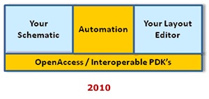
Traditional approach is sequential: Schematic then Layout.
Now a parallel approach with Agile Layout, parallel.

GUI – our own.
IPL Initiative -Analog Constraints in place, we follow, not that active. Original contributor to IPL.
Example: 40,000 devices with TSMC 28nm took just 8 days with Cira Nova tools. Very experienced user, 3 months to get that skill. 1 week to get user efficient.
Both circuit designers doing own placement then layout team does routing. Other places have IC layout designers.
Funding – privately held, both VC and corporate investors.
Direct sales. Korea and Taiwan have distributors, and office in the UK.
Success in 2013 – continued chip tape outs, larger chips, better silicon. More public names. CSR.
Mostly 40nm and 28nm AMS, even 20nm designs. Memory customer.
(Cadence – show me the GXL tapeouts)
IDMs and fabless using tool, but won’t allow disclosudre.
Who is using your tools? Stay tuned because of confidentiality.
Summary
I got into EDA back in 1986 with Silicon Compilers because I believed in their correct by construction approach to chip design and IC layout. Now I see Ciranova on a similar path of automation where the custom layout results are correct by construction. The days of tweaking IC layout by hand are going the way of calligraphy, it’s very pretty but not too practical.
Full disclosure: I consulted for Ciranova in 2011.


Captain America: Can Elon Musk Save America’s Chip Manufacturing Industry?