I have written before about eSilicon taking their internal quoting tool and making it user accessible. This first started just for MPW shuttles for half-a-dozen foundries, and then was extended to cover production runs at TSMC. And it is getting heavily used; eSilicon have had 315 people register to use it from 43 different countries… Read More

Tag: tsmc
A Complete Scalable Solution for IP Signoff
In an SoC world driven by IP, where an SoC can have hundreds of IP (sourced not only from 3[SUP]rd[/SUP] party but also from internal business units which can have a lot of legacy) integrated together, it has become essential to have a comprehensive and standard method to verify and signoff the IP. Additionally, these checks must … Read More
TSMC Breaks More Records in Q3 2014!
As previously predicted TSMC is having another record breaking SoC quarter. TSMC is my favorite economic bellwether and from what I can see the semiconductor industry will continue to grow this year and next at a rapid rate thanks to TSMC and the fabless semiconductor ecosystem:
We have set a new record of revenue and profitability… Read More
TSMC ♥ Cadence!
One of the questions I routinely ask amongst the fabless semiconductor ecosystem is, “How are the EDA vendors doing?” There are always complaints because, let’s face it, we all like to complain. On occasion however I do hear about a vendor who goes above and beyond the call of duty and it really brightens my day.
Of late,… Read More
Intel Invades China Mobile Market!
As you may have heard, Intel is making some interesting moves into the China mobile market. At first it had me a bit puzzled but I had some lengthy discussions about it during ARM TechCon last week so I’m ready to start writing. Spoiler alert: This will be pro Intel so please sit down and take some deep breaths before reading.
The first… Read More
The Apple Samsung TSMC Intel 14nm Mashup!
One of the strengths of the fabless semiconductor ecosystem is competition since it keeps innovation high and prices low. One of the challenges of fostering competition is that you have to make good on a threat of using a competing product during a pricing negotiation. Well, in my opinion, for the next version of the iPhone, Apple… Read More
ARM ♥ TSMC!
This week is the 10[SUP]th[/SUP] annual ARM Technical Conference in Silicon Valley. In regards to size, content, and relevance, I believe ARM TechCon is the #1 event for the fabless semiconductor ecosystem for sure. I attended keynotes, sessions, and walked the hallways on Wednesday and Thursday. I wish I could write about everything… Read More
ANSYS Tools Shine at FinFET Nodes!
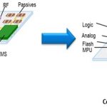
In the modern semiconductor ecosystem we are seeing rapid advancement in technology breaking past once perceived limits; 28nm, 20nm, 16-14nm, 10nm and we are foreseeing 7nm now. Double and multi-patterning are already being seen along with complex FinFET structures in transistors to gain the ultimate advantages in PPA from… Read More
Who Will Lead at 10nm?
There has been a lot of discussion on SemiWiki lately around 14nm FinFET technology and who really leads and by how much. I thought it would be interesting to review some process metrics for previous technology generation and then make some forecasts around 10nm.
The focus of this article will be Intel, TSMC and Global Foundries/Samsung… Read More
ARM ♥ Xilinx!
The good news is that as a part of SemiWiki we get free media passes to all of the cool conferences. The bad news is that our inboxes get flooded with announcements. ARM TechCon is next week and my delete button is on overtime but it is interesting to see who is active in conferences and who is not. In this case Xilinx is very active and Altera… Read More