You are currently viewing SemiWiki as a guest which gives you limited access to the site. To view blog comments and experience other SemiWiki features you must be a registered member. Registration is fast, simple, and absolutely free so please,
join our community today!
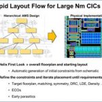
Ciranova presented a hierarchical custom layout flow used on several large advanced-node designs to reduce total layout time by about 50%. Ciranova itself does automated floorplanning and placement software with only limited routing; but since the first two constitute the majority of custom layout time, and strongly influence… Read More
Ever since the “Intel Reinvents Transistors Using New 3-D Structure” PR campaign I have been at odds with them. As technologists, I have nothing but respect for Intel. The Intel PR department, however, quite frankly, is evil. Correct me if I’m wrong here but Intel did not “reinvent” the transistor. Nor did they come up with the name… Read More
Having spent a considerable amount of time with Solido, they were one of the founding members of SemiWiki, I can tell you that at 20nm the Variation Designer Platform is a critical part of the emerging 20nm design methodology. You can read more on Solido’s SemiWiki landing page HERE. It is well worth the click.
With technology… Read More
Now that the 28nm challenges are dead
It is time to look ahead
The tabloid pundits may not agree
But Moore’s law again you will see
The semiconductor ecosystem is humming
(2X gate density -20%+ performance-20%+ power savings)
The 20nm design starts are coming!
Okay, I’m really bad at poetry. Gambling however, I do pretty well. Las… Read More
There is an interesting discussion in the SemiWiki forum in response to the EETimes article: Intel exec says fabless model ‘collapsing’. Definitely an interesting debate, one worth our time since the advertising click hungry industry pundits will certainly jump all over it. Clearly I’m biased since I helped build… Read More
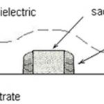
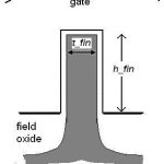
The previous post in this series provided an overview of FinFET devices. This article will briefly cover FinFET fabrication.
The major process steps in fabricating silicon fins are shown in Figures 1 through 3. The step that defines the fin thickness uses Sidewall Image Transfer (SIT). Low-pressure chemical vapor (isotropic)… Read More
The biggest news out of the TSMC Symposium last week was the 20nm update. Lots of debate and speculation, just why is TSMC releasing one version of 20nm (20nm SoC) versus multiple versions like in 40nm (LP, G, LPG) and 28nm (HP, HPM, HPL, LP)? Here are my thoughts, I would also be interested in your feedback in the comment section. This… Read More
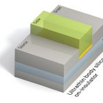
This is the first of a multi-part series, to introduce FinFET technology to SemiWiki readers. These articles will highlight the technology’s key characteristics, and describe some of the advantages, disadvantages, and challenges associated with this transition. Topics in this series will include FinFET fabrication,… Read More
It was an honor to see DR. Chenming Huspeak and to learn more about FinFets, a technology he has championed since 1999. Chenming is considered an expert on the subject and is currently a TSMC Distinguished Professor of Microelectronics at University of California, Berkeley. Prior to that he was the Chief Technology Officer of TSMC.… Read More
Ever since the TSMC OIP Forum where Dr. Shang-Yi Chiang openly asked customers, “When do you want 3D Transistors (FinFETS)?” I have heard quite a few debates on the topic inside the top fabless semiconductor companies. The bottom line, in my expert opinion, is that TSMC will add FinFETS to the N20 (20nm) process node in parallel with… Read More