You are currently viewing SemiWiki as a guest which gives you limited access to the site. To view blog comments and experience other SemiWiki features you must be a registered member. Registration is fast, simple, and absolutely free so please,
join our community today!
"The Year of the eFPGA" 2017 Recapby Tom Dillinger on 12-22-2017 at 7:00 amCategories: eFPGA, Flex Logix, FPGA, IP
This past January, I had postulated that 2017 would be the “Year of the Embedded FPGA”, as a compelling IP offering for many SoC designs (link). As the year draws to a close, I thought it would be interesting to see how that prediction turned out.
The criteria that would be appropriate metrics include: increasing capital investment;… Read More
Semiconductor IP is the fastest growing market inside the fabless ecosystem, it always has been and always will be, especially now that non-traditional chip companies are quickly entering the mix. Towards the end of the year I always talk to the ecosystem to see what next year has in store for us and 2018 looks to be another year of … Read More
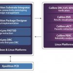
Chip designers are familiar with the additional physical design checking requirements that were incorporated into flows at advanced process nodes. With the introduction of optical correction and inverse lithography technology applied during mask data generation, and with the extension of a 193nm exposure source to finer… Read More
Large SoC design teams typically have a cadre of project managers to oversee all facets of functional verification — e.g., specification, reviews, directed testbench development, automated (pseudorandom) testcase generation, HDL coverage measurement and reporting, and bug identification/tracking database management.… Read More
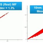
Extraction Features for 7nmby Tom Dillinger on 08-21-2017 at 12:00 pmCategories: Cadence, EDA, FinFET
Frequent Semiwiki readers are familiar with the importance of close collaboration between the foundries and EDA tool developers, to provide the crucial features required by new process nodes. Perhaps the best illustration of the significance of this collaboration is the technical evolution of layout parasitic extraction.… Read More
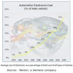
Semiwiki readers are no doubt very familiar with the increasing impact of the automotive market on the semiconductor industry. The magnitude and complexity of the electronic systems that will be integrated into upcoming vehicle designs reflects the driver automation, safety, and entertainment features that are in growing… Read More
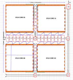
A key application for embedded FPGA (eFPGA) technology is to provide functionality for specific algorithms — as the throughput of this implementation exceeds the equivalent code executing on a processor core, these SoC blocks are often referred to as accelerators. The programmability of eFPGA technology offers additional… Read More
Regular Semiwiki readers are aware of the rapid emergence of various (multi-die) advanced package technologies, such as: FOWLP (e.g., Amkor’s SWIFT, TSMC’s InFO); 2D die placement on a rigid substrate (e.g., TSMC’s CoWoS); and, 2.5D “stacked die” with vertical vias (e.g., any of the High Bandwidth Memory,… Read More
There is an emerging set of advanced packaging technologies that enables unique product designs, with the capability to integrate multiple die, from potentially heterogeneous technologies. These “system-in-package” (SiP) offerings provide architects with the opportunity to optimize product performance, power, cost,… Read More
Regular Semiwiki readers are aware that embedded FPGA (eFPGA) IP development is a rapidly growing (and evolving) technical area. The applications for customizable and upgradeable logic in the field are many and diverse — as a result, improved performance, greater configurable logic capacity/density, and comprehensive… Read More