You are currently viewing SemiWiki as a guest which gives you limited access to the site. To view blog comments and experience other SemiWiki features you must be a registered member. Registration is fast, simple, and absolutely free so please,
join our community today!
Timing closure is one of the most challenging aspects of ASIC design. While traditionally seen as a backend process, its resolution begins at the architectural level and extends through the implementation stages. This webinar examines the key obstacles designers encounter and demonstrates how our timing closure solutions
…
Read More
Near the end of any large SoC design project, the RTL code is nearly finished, floorplanning has been done, place and route has a first-pass, static timing has started, but the timing and power goals aren’t met. So, iteration loops continue on blocks and full-chip for weeks or even months. It could take a design team 5-7 days… Read More
Cadence invests heavily in the development of their Tempus Timing Signoff Solution due to its importance in the SoC design flow. I recently had a discussion on the topic of the most recent Tempus update with Brandon Bautz, senior product management group director in the Digital & Signoff Group, and Hitendra Divecha, product… Read More
The old adage that goes the one constant thing you can always count on is change, could easily be reworded for semiconductor design to say the one constant thing you can count on is variation. This is doubly true. Not only is variation, in all its forms, a constant factor in design, additionally the methods of analyzing and dealing … Read More
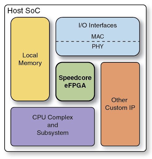
Once the benefits of using an embedded FPGA fabric are understood, the next question is about how timing closure is handled between the ASIC and the eFPGA blocks. First let’s look briefly at the advantages. By moving the eFPGA on to the SOC die, tons of I/O logic and the need for any package and board interconnect will vanish. Package… Read More
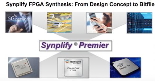
You might wonder why, in FPGA design, you would go beyond simply using the design tools provided by the FPGA vendor (e.g. Xilinx, Intel/Altera and Microsemi). After all, they know their hardware platform better than anyone else, and they’re pretty good at design software too. But there’s one thing none of these providers want to… Read More
The appeal of embedding an FPGA IP in an ASIC design is undeniable. For much of your design, you want all the advantages of ASIC: up to GHz performance, down to mW power (with active power management), all with very high levels of integration with a broad range of internal and 3[SUP]rd[/SUP]-party IP (analog/RF, sensor fusion, image/voice… Read More
Timing closure is the perennial issue in digital IC design. While the specific problem that has needed to be solved to achieve timing closure over the decades has continuously changed, it has always been a looming problem. And the timing closure problem has gotten more severe with 16/14nm FinFET SoCs due to greater distances between… Read More
The challenge of tracking design progress is a shared problem for individual designers, team leaders, and project managers. At each level the ability to step back from just reviewing error log files and seeing the arc of the whole design as it moves forward is valuable. The difficulty of seeing the whole picture is exacerbated when… Read More
Timing closure is a “tortoise” for some system-on-chip (SoC) designers just the way many digital guys call RF design a “black art”. Chip designers often tell horror stories of doing up to 20 back-end physical synthesis place & route (SP&R) iterations with each iteration taking a week or more. “Timing closure”, a largely… Read More


