You are currently viewing SemiWiki as a guest which gives you limited access to the site. To view blog comments and experience other SemiWiki features you must be a registered member. Registration is fast, simple, and absolutely free so please,
join our community today!
My engineering background includes designing at the transistor-level, so I was drawn to attend a webinar today presented by Tanner EDAand Incentia about Adding a Digital Block to an Analog Design. Many of the 30,000 users of Tanner tools have been doing AMS designs, so adding logic synthesis and static timing analysis from Incentia… Read More
First thing at DACtoday I met with Greg Lebsack of Tanner EDA to ask about what’s new in the past year for his EDA company. Here are my meeting notes, so there’s not much prose for my DAC blogs this year.
… Read More
The generosity of the fabless semiconductor ecosystem never ceases to amaze me. Paul McLellan and I wrote a book for the greater good and now key members of our industry will make sure that 1,500 people at this year’s Design Automation Conference will get copies. As a special thank you to all of our supporters SemiWiki will be hosting… Read More
Tanner EDA is making waves at their customer’s sites as the mixed-signal design suite from Tanner EDA, Incentia Design Systems, Inc. and Aldec, Inc. helps ASIC Design House lower cost and increase efficiency with no compromise in performance. In today’s ‘always on’, Internet of Things connected world, the demand for high-performance,… Read More
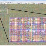
IC place and route tools can be very high-priced EDA software to purchase or lease, so there’s some good news for AMS designers that need an affordable digital place and route tool for their mostly analog designs. Today the team at Tanner EDAannounced a totally new place and route system has been added to their Schematic Driven… Read More
Wearables are going to be a real game changer for the fabless semiconductor ecosystem, absolutely. What other high volume semiconductor market segment has such a low barrier of entry? Speaking of low barrier of entry, the first stop on my Southern California trip last week was Monrovia, the home of Tanner EDA. Tanner is already … Read More
IC designers use EDA tools to implement their logical and physical design, and these tools require foundry-specific information for:
- Design Rule Checking (DRC)
- Layout Versus Schematic (LVS)
- Library Symbols
- Parasitic EXtraction (PEX)
…
Read More
My background includes transistor-level IC design, so I take delight in talking with engineers like Dr. Lanny Lewyn that are still practicing the art and science of analog IC design. Dr. Lewynis a Life Senior Member of the IEEE and has a consulting business. If you live in Santa Clara, then consider attending a live seminar on October… Read More
Competition in EDA is absolutely necessary in order for the fabless semiconductor ecosystem to thrive. AMS tools with a low learning curve, high interoperability, and a powerful user interface improve design team productivity and enable a low total cost of ownership. That is why Tanner EDA has shipped over 33,000 licenses of … Read More
With nearly twenty five years in business, Tanner EDA Application Engineers have seen a wide range of support requests. One consistent topic area is around design data management and design reuse. In one recent instance, our customer, an IDM who produces imaging sensors for infrared vision systems, called on Tanners AE team for… Read More