Some post-silicon bugs are unavoidable, but we’re getting better at catching them before we ship. Here we look at a method based on a bare-metal exerciser to stress-test the MMU. Paul Cunningham (GM, Verification at Cadence), Raúl Camposano (Silicon Catalyst, entrepreneur, former Synopsys CTO and lecturer at Stanford, EE292A)… Read More
Tag: synopsys
Scaling Multi-Die Connectivity: Automated Routing for High-Speed Interfaces
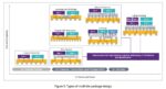
This article concludes the three-part series examining key methodologies required for successful multi-die design. The first article Reducing Risk Early: Multi-Die Design Feasibility Exploration focused on feasibility exploration and early architectural validation, while the second article Building the Interconnect… Read More
Agentic AI and the Future of Engineering
Agentic AI emerges in this Synopsys Converge keynote not as a futuristic add-on, but as a practical response to the growing complexity of engineering. In the speaker’s view, the traditional way of designing chips, systems, and intelligent products is no longer sufficient for the era of physical AI. Engineers are now dealing with… Read More
Efficient Bump and TSV Planning for Multi-Die Chip Designs
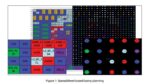
The semiconductor industry has experienced rapid advancements in recent years, particularly with the increasing demand for high-performance computing, artificial intelligence, and advanced automotive systems. Traditional single-die chip designs are often unable to meet modern PPA requirements. As a result, engineers… Read More
Reducing Risk Early: Multi-Die Design Feasibility Exploration
The semiconductor industry is entering a new era in system design. As traditional monolithic scaling approaches its economic and physical limits, multi-die architectures are emerging as a primary pathway for delivering continued improvements in performance, power efficiency, and integration density. By distributing … Read More
Building the Interconnect Foundation: Bump and TSV Planning for Multi-Die Systems
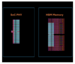
The first article in this series examined how feasibility exploration enables architects to evaluate multi-die system configurations while minimizing early design risk. Once architectural decisions are validated, designers must translate conceptual connectivity requirements into physical interconnect infrastructure.… Read More
How Customized Foundation IP Is Redefining Power Efficiency and Semiconductor ROI
As computing expands from data centers to edge devices, semiconductor designers face increasing pressure to optimize both performance and energy efficiency. Advanced process nodes continue to provide transistor-level improvements, but scaling alone cannot meet the demands of hyperscale AI infrastructure or ultra-low-power… Read More
Designing the Future: AI-Driven Multi-Die Innovation in the Era of Agentic Engineering
At the 2026 Chiplet Summit, Synopsys presented a bold vision for the future of semiconductor innovation: AI-driven multi-die design powered by agentic intelligence. As the semiconductor industry shifts rapidly toward chiplet-based architectures and 3D stacking, the complexity of design, verification, and system integration… Read More
Hardware is the Center of the Universe (Again)
The 40-Year Evolution of Hardware-Assisted Verification — From In-Circuit Emulation to AI-Era Full-Stack Validation
For more than a decade, Hardware-Assisted Verification platforms have been the centerpiece of the verification toolbox. Today, no serious semiconductor program reaches tapeout without emulation or FPGA-prototyping… Read More
Accelerating Static ESD Simulation for Full-Chip and Multi-Die Designs with Synopsys PathFinder-SC
As analog and mixed-signal designs become increasingly complex, parasitic effects dominate both design time and cost, consuming 30–50% of engineers’ effort in debugging and reanalyzing circuits. Addressing these multiphysics effects requires early verification strategies and reliable simulation solutions. Modern … Read More